
Texas Instruments
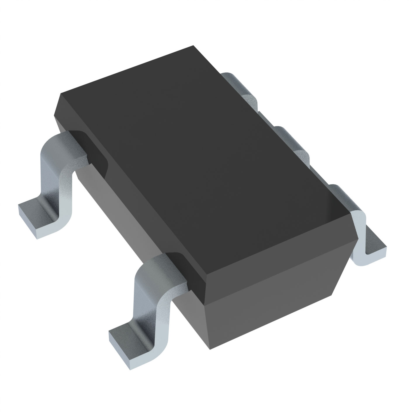
OPA354AQDBVRQ1
OP Amps, Buffer Amps ICs


.png?x-oss-process=image/format,webp/resize,p_30)


OPA354AQDBVRQ1 Description
The Texas Instruments OPA354AQDBVRQ1 is a high-performance, low-noise, low-power operational amplifier (op-amp) designed for a wide range of applications. Here's a description of the model, its features, and potential applications:
Model Description:
The OPA354AQDBVRQ1 is a precision operational amplifier offered in a compact Quad Flat No-Lead (QFN) package. It is designed to provide excellent performance in terms of speed, accuracy, and power efficiency, making it suitable for a variety of precision analog signal processing tasks.
Features:
- Low Input Noise: The OPA354AQDBVRQ1 features a low input voltage noise of 2.2 nV/√Hz, which is beneficial for applications requiring high signal-to-noise ratios.
- Low Power Consumption: It operates with a low supply current of 1.95 mA (typical), making it suitable for battery-powered and portable applications.
- Wide Supply Voltage Range: The device can operate with a supply voltage range of 2.7 V to 10.8 V, providing flexibility in system design.
- High Input Impedance: The op-amp has a high input impedance, which is ideal for driving capacitive loads and minimizing the loading effect on the input signal.
- Low Output Drift: The OPA354AQDBVRQ1 exhibits low output voltage drift, which is crucial for maintaining signal integrity over time and temperature variations.
- High Slew Rate: A slew rate of 1.2 V/µs allows the device to handle fast-changing input signals without significant distortion.
- Rail-to-Rail Input and Output: The op-amp can operate with input and output signals that go close to the supply rails, which is useful for single-supply applications.
- Short-Circuit Protection: The device includes internal protection against short-circuit conditions, enhancing its reliability and robustness.
Applications:
- Audio Amplification: The low noise and high linearity make the OPA354AQDBVRQ1 suitable for audio preamplifiers and line drivers.
- Medical Instruments: The precision and low drift characteristics are ideal for medical equipment that requires accurate signal processing, such as patient monitoring systems and diagnostic devices.
- Sensor Conditioning: The OPA354AQDBVRQ1 can be used to amplify and filter signals from sensors in industrial and automotive applications.
- Battery Monitors: The low power consumption and precision make it suitable for battery monitoring circuits in portable devices and energy harvesting systems.
- Data Acquisition Systems: The device can be used in the front-end signal conditioning for data acquisition systems, providing accurate amplification and filtering of sensor signals.
- Precision DC and AC Gain Blocks: The OPA354AQDBVRQ1 can be used to create high-precision gain blocks for various signal conditioning applications.
- Strains Gauge Conditioning: The low noise and high accuracy of the op-amp make it suitable for conditioning signals from strain gauges in force and pressure measurement applications.
The OPA354AQDBVRQ1 is a versatile operational amplifier that can be integrated into a wide range of precision analog signal processing applications, benefiting from its low noise, low power consumption, and high performance characteristics.
Tech Specifications
OPA354AQDBVRQ1 Documents
Download datasheets and manufacturer documentation for OPA354AQDBVRQ1
 OPA354, 2354(A), 4354(A)-Q1
  OPA354, 2354(A), 4354(A)-Q1
  OPA4354 17/Jul/2018 OPA Rev. 11/Aug/2016
 Shopping Guide


.png?x-oss-process=image/format,webp/resize,h_32)


