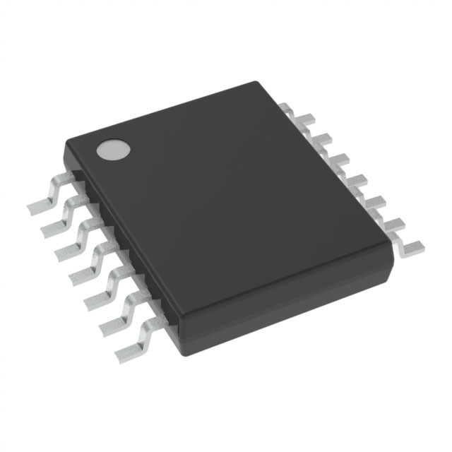
Texas Instruments_OPA4172AQPWRQ1

Texas Instruments
OPA4172AQPWRQ1  
OP Amps, Buffer Amps ICs

Texas Instruments
OPA4172AQPWRQ1
687-OPA4172AQPWRQ1
Ersa
Texas Instruments-OPA4172AQPWRQ1-datasheets-13489256.pdf
IC OPAMP GP 4 CIRCUIT 14TSSOP
In Stock : 1350

Not available to buy online? Want the lower wholesale price? Please Send RFQ to get best price, we will respond immediately

QUICK RFQ
ADD TO RFQ LIST
ersa FreeSample ersa flow
  • Quantity
  • Unit Price
  • Ext. Price
    • 1+
    • $5.18825
    • $5.19
    • 10+
    • $4.55069
    • $45.51
    • 30+
    • $4.16318
    • $124.9
    ADD TO CART
    QUICK ORDER
    $5.18825    $5.19
    ISO9001
    Quality Policy
    ISO45001
    ISO14001

    OPA4172AQPWRQ1 Description

    The OPA4172AQPWRQ1 is a precision operational amplifier (op-amp) from Texas Instruments. It is designed to provide high precision and low noise performance in a wide range of applications.

    Description:

    The OPA4172AQPWRQ1 is a single, precision operational amplifier with a low input offset voltage and drift, low input bias and offset currents, and low noise. It is available in a compact 8-pin QFN package.

    Features:

    • Low input offset voltage: 200µV max
    • Low input bias current: 1pA max
    • Low input offset current: 0.5pA max
    • Low noise: 7nV/√Hz
    • Wide supply voltage range: 2.5V to 36V
    • High output current: ±100mA
    • Unity-gain stable
    • Available in 8-pin QFN package

    Applications:

    The OPA4172AQPWRQ1 is suitable for a wide range of precision applications, including:

    • Data acquisition systems
    • Medical instrumentation
    • Strain gauge amplifiers
    • pH measurement systems
    • Pressure sensor amplifiers
    • Precision DC gain applications
    • Audio applications
    • Battery monitors

    In summary, the OPA4172AQPWRQ1 is a precision operational amplifier from Texas Instruments that offers low input offset voltage and drift, low input bias and offset currents, and low noise. It is suitable for a wide range of precision applications, including data acquisition systems, medical instrumentation, and audio applications.

    Tech Specifications

    Voltage - Supply Span (Max)
    Number of Channels per Chip
    Power Supply Type
    Maximum Input Offset Voltage (mV)
    PPAP
    Gain Bandwidth Product
    Product Status
    Current - Input Bias
    Automotive
    Maximum Input Offset Current (uA)
    Rail to Rail
    Supplier Package
    Package / Case
    Typical Voltage Gain (dB)
    REACH Status
    Typical Input Bias Current (uA)
    EU RoHS
    Amplifier Type
    Maximum Dual Supply Voltage (V)
    Moisture Sensitivity Level (MSL)
    Typical Input Noise Voltage Density (nV/rtHz)
    Operating Temperature
    Typical Slew Rate (V/us)
    ECCN
    Grade
    Supplier Temperature Grade
    Mounting Type
    Current - Supply
    Standard Package Name
    Pin Count
    Shut Down Support
    Mounting
    Qualification
    Minimum Single Supply Voltage (V)
    Minimum PSRR (dB)
    Typical Dual Supply Voltage (V)
    Voltage - Supply Span (Min)
    Lead Shape
    SVHC
    Manufacturer Type
    HTSUS
    Package
    Current - Output / Channel
    Minimum CMRR (dB)
    Maximum Quiescent Current (mA)
    PCB changed
    Output Type
    HTS
    ECCN (US)
    Supplier Device Package
    Minimum CMRR Range (dB)
    Minimum Operating Temperature (°C)
    Maximum Operating Temperature (°C)
    Process Technology
    Typical Gain Bandwidth Product (MHz)
    Package Height
    Mfr
    RoHS Status
    Maximum Input Bias Current (uA)
    Typical Noninverting Input Current Noise Density (pA/rtHz)
    Slew Rate
    Package Length
    Minimum Dual Supply Voltage (V)
    Voltage - Input Offset
    Series
    Type
    Maximum Single Supply Voltage (V)
    Part Status
    Number of Circuits
    Package Width
    Typical Settling Time (ns)
    Base Product Number
    Maximum Dual Supply Voltage
    Unit Weight
    3 dB Bandwidth
    en - Input Voltage Noise Density
    Vos - Input Offset Voltage
    Minimum Dual Supply Voltage
    Product
    RoHS
    Supply Voltage - Min
    THD plus Noise
    Operating Supply Current
    SR - Slew Rate
    Number of Channels
    Development Kit
    Maximum Operating Temperature
    Ib - Input Bias Current
    Supply Voltage - Max
    Mounting Style
    Input Type
    Minimum Operating Temperature
    CMRR - Common Mode Rejection Ratio
    In - Input Noise Current Density
    Ios - Input Offset Current
    Shutdown
    Moisture Sensitive
    Output Current per Channel
    USHTS
    GBP - Gain Bandwidth Product

    OPA4172AQPWRQ1 Documents

    Download datasheets and manufacturer documentation for OPA4172AQPWRQ1

    Ersa Signal e-Book: OP Amp Design Topics       OPA2172-Q1, OPA4172-Q1 Datasheet      
    Ersa Device Symbolization Change 13/Jun/2023      
    Ersa OPA2172-Q1, OPA4172-Q1 Datasheet      
    Ersa Design 22/Feb/2022      

    Shopping Guide

    Payment Methods
    Payment Methods include Prepayment TT (bank transfer), Western Union, and PayPal. Customers are responsible for shipping costs, bank charges, customs duties and taxes.
    Shipping Rate
    Shipments are made once a day around 5pm, excluding Sundays. Once shipped, the estimated delivery time is usually 5-7 business days, depending on the courier you choose.
    Delivery Methods
    Provide DHL, FedEx, UPS, EMS, SF Express and Registered Airmail International Delivery Service