
 German
 Japanese
 Portuguese
 Korea
Korea
 Mexico
 Dutch
Dutch


Texas Instruments
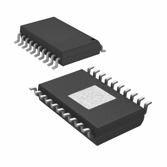
OPA564AQDWPRQ1

Why Choose Us?
Professional Platform
B2B & B2C purchasingDelivery at full speed
1-2 days deliveryWide variety
Original manufacturers365 days guarantee
Responsible quality
.png)


Tech Specifications
OPA564AQDWPRQ1 Description
The OPA564AQDWPRQ1 is a high-performance, low-noise, low-power, precision operational amplifier (op-amp) from Texas Instruments. It is designed for use in a wide range of applications that require high precision and low noise performance.
Description:
The OPA564AQDWPRQ1 is a monolithic JFET input operational amplifier that features a high input impedance, low input offset voltage, and low input bias current. It is available in a small-outline wide (SOW) package and is designed for use in a wide range of applications that require high precision and low noise performance.
Features:
- High input impedance: The OPA564AQDWPRQ1 has a high input impedance, which makes it suitable for use in applications where the input signal source has a high output impedance.
- Low input offset voltage: The OPA564AQDWPRQ1 has a low input offset voltage, which ensures accurate amplification of the input signal.
- Low input bias current: The OPA564AQDWPRQ1 has a low input bias current, which minimizes the loading effect on the input signal source.
- Low noise: The OPA564AQDWPRQ1 has a low noise performance, making it suitable for use in applications that require high precision and low noise performance.
- Precision: The OPA564AQDWPRQ1 is designed for use in precision applications that require high accuracy and low distortion.
Applications:
The OPA564AQDWPRQ1 is suitable for use in a wide range of applications that require high precision and low noise performance. Some of the common applications include:
- Audio equipment: The OPA564AQDWPRQ1 can be used in audio equipment such as preamplifiers, equalizers, and active filters.
- Medical equipment: The OPA564AQDWPRQ1 can be used in medical equipment such as patient monitoring systems and medical imaging systems.
- Measurement and control systems: The OPA564AQDWPRQ1 can be used in measurement and control systems that require high precision and low noise performance.
- Instrumentation: The OPA564AQDWPRQ1 can be used in instrumentation such as oscilloscopes, spectrum analyzers, and signal generators.
In summary, the OPA564AQDWPRQ1 is a high-performance, low-noise, low-power, precision operational amplifier that is suitable for use in a wide range of applications that require high precision and low noise performance. Its high input impedance, low input offset voltage, and low input bias current make it an ideal choice for use in applications where the input signal source has a high output impedance.
FAQ
| Quantity | Unit Price | Ext. Price |
|---|---|---|
| 1+ | $6.21428 | $6.21 |
| 10+ | $5.34515 | $53.45 |
| 30+ | $4.81372 | $144.41 |
| 100+ | $4.36972 | $436.97 |
Not available to buy online? Want the lower wholesale price? Please Send RFQ to get best price, we will respond immediately


.png?x-oss-process=image/format,webp/resize,h_32)


