
 German
 Japanese
 Portuguese
 Korea
Korea
 Mexico
 Dutch
Dutch


Why Choose Us?
Professional Platform
B2B & B2C purchasingDelivery at full speed
1-2 days deliveryWide variety
Original manufacturers365 days guarantee
Responsible quality
.png)


Tech Specifications
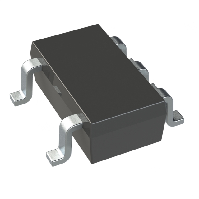
OPA607QDBVRQ1 Description
The Texas Instruments OPA607QDBVRQ1 is a high-performance operational amplifier (op-amp) that is designed for a wide range of precision applications. Here is a description of the model, its features, and potential applications:
Description:
The OPA607QDBVRQ1 is a precision operational amplifier that is part of Texas Instruments' portfolio of high-quality analog signal processing components. It is available in a compact Quad Flat No-Lead (QFN) package, making it suitable for space-constrained applications. This op-amp is designed to provide excellent DC and AC performance characteristics, making it ideal for a variety of precision applications.
Features:
-
Low Input Offset Voltage: The OPA607QDBVRQ1 has a very low input offset voltage, which is crucial for maintaining precision in signal processing applications.
-
Low Input Bias Current: It features a low input bias current, which helps to minimize the loading effect on the input signal source, preserving the integrity of the input signal.
-
High Slew Rate: The device has a high slew rate, allowing it to respond quickly to fast-changing input signals without significant distortion.
-
Low Noise: The OPA607QDBVRQ1 is designed to operate with low noise, which is essential for applications where signal-to-noise ratio is critical.
-
Wide Supply Voltage Range: It can operate over a wide range of supply voltages, making it versatile for different power supply configurations.
-
High Output Drive Capability: The op-amp can drive a wide range of loads, making it suitable for driving capacitive loads or driving the input of other stages in a signal chain.
-
Temperature Stability: The device maintains its performance across a wide temperature range, making it suitable for applications where the operating environment can vary significantly.
-
Robustness: It is designed to be robust against various types of interference, such as supply voltage noise and electromagnetic interference (EMI).
Applications:
-
Precision Measurement Systems: Due to its low offset voltage and drift, the OPA607QDBVRQ1 is ideal for use in precision measurement systems where accurate amplification of small signals is required.
-
Data Acquisition Systems: It can be used in data acquisition systems to amplify and filter signals before they are digitized by an analog-to-digital converter (ADC).
-
Medical Instruments: The precision and low noise characteristics make it suitable for medical instruments where signal integrity is critical, such as in electrocardiogram (ECG) machines or other bio-signal processing applications.
-
Audio Equipment: In high-fidelity audio equipment, the OPA607QDBVRQ1 can be used to provide clean amplification of audio signals.
-
Sensor Conditioning: It can be used to condition signals from various types of sensors, such as temperature, pressure, or strain gauges, where accurate signal processing is essential.
-
Industrial Control Systems: For applications in industrial control systems where reliable and precise signal amplification is needed, the OPA607QDBVRQ1 is a suitable choice.
-
Communication Systems: In communication systems, it can be used for signal processing tasks such as filtering and amplification of signals before transmission or after reception.
-
Automotive Applications: The device's robustness and temperature stability make it suitable for automotive applications where it can be used for signal conditioning in various sensors and control systems.
The OPA607QDBVRQ1 is a versatile operational amplifier that, with its combination of precision and robustness, can be applied across a wide range of demanding signal processing tasks.
FAQ
Not available to buy online? Want the lower wholesale price? Please Send RFQ to get best price, we will respond immediately


.png?x-oss-process=image/format,webp/resize,h_32)


