
Texas Instruments
OPA863ADBVR
OP Amps, Buffer Amps ICs


.png?x-oss-process=image/format,webp/resize,p_30)


OPA863ADBVR Description
OPA863ADBVR Description
The OPA863ADBVR is a single-channel, high-precision operational amplifier from Texas Instruments, designed for demanding applications that require high performance and reliability. This op-amp is part of the OPAx863A series and is optimized for high-speed, low-distortion signal processing. It features a wide supply voltage range, from 2.7 V to 12.6 V, making it suitable for a variety of power supply configurations. The OPA863ADBVR boasts a gain bandwidth product of 50 MHz and a -3dB bandwidth of 105 MHz, ensuring high-frequency performance with minimal signal degradation. Its slew rate of 100 V/µs allows for rapid response to input changes, making it ideal for applications requiring fast signal processing.
OPA863ADBVR Features
- High Precision and Performance: The OPA863ADBVR offers a low input bias current of 300 nA and an input offset voltage of 10 µV, ensuring high precision in signal amplification. These characteristics make it suitable for applications where accuracy and stability are critical.
- Wide Supply Voltage Range: With a supply voltage range of 2.7 V to 12.6 V, the OPA863ADBVR can operate in diverse power supply environments, providing flexibility in system design.
- High-Speed Operation: The amplifier's 50 MHz gain bandwidth product and 105 MHz -3dB bandwidth enable it to handle high-frequency signals efficiently. The 100 V/µs slew rate ensures rapid response to input changes, making it ideal for high-speed applications.
- Low Power Consumption: The OPA863ADBVR operates with a supply current of only 800 µA, making it energy-efficient without compromising performance.
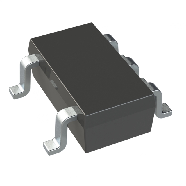
- Surface Mount Packaging: The device is available in a surface mount package, facilitating easy integration into compact and high-density PCB designs.
- Compliance and Reliability: The OPA863ADBVR is REACH unaffected and RoHS3 compliant, ensuring it meets environmental and safety standards. It also has a moisture sensitivity level (MSL) of 1 (unlimited), making it suitable for various manufacturing environments.
- Single-Channel Design: The single-channel configuration simplifies circuit design and reduces complexity, while still delivering high performance.
OPA863ADBVR Applications
The OPA863ADBVR is well-suited for a variety of applications that demand high precision and high-speed signal processing. Some specific use cases include:
- High-Frequency Signal Processing: Ideal for applications such as RF signal amplification, where high-frequency response and low distortion are critical.
- Precision Measurement Equipment: Suitable for precision instruments that require accurate and stable signal amplification, such as oscilloscopes and spectrum analyzers.
- Medical Devices: Can be used in medical imaging and diagnostic equipment where high precision and reliability are essential.
- Industrial Automation: Applicable in control systems and sensors that require fast response times and high accuracy.
- Telecommunications: Useful in communication systems where high-speed signal processing and low distortion are necessary.
Conclusion of OPA863ADBVR
The OPA863ADBVR from Texas Instruments is a high-precision, single-channel operational amplifier that excels in high-speed and low-distortion signal processing. Its wide supply voltage range, low power consumption, and compliance with environmental standards make it a versatile and reliable choice for a variety of applications. Whether used in high-frequency signal processing, precision measurement equipment, or industrial automation, the OPA863ADBVR delivers exceptional performance and reliability. Its unique combination of high-speed operation, low input bias current, and low input offset voltage sets it apart from similar models, making it an ideal choice for demanding applications in the electronics industry.
Tech Specifications
OPA863ADBVR Documents
Download datasheets and manufacturer documentation for OPA863ADBVR
 OPAx863A
 Shopping Guide


.png?x-oss-process=image/format,webp/resize,h_32)


