
 German
 Japanese
 Portuguese
 Korea
Korea
 Mexico
 Dutch
Dutch


Texas Instruments
SN54F11J

Why Choose Us?
Professional Platform
B2B & B2C purchasingDelivery at full speed
1-2 days deliveryWide variety
Original manufacturers365 days guarantee
Responsible quality
.png)


Tech Specifications
SN54F11J Description
SN54F11J Description
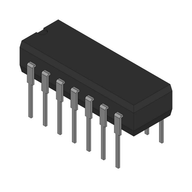
The SN54F11J is a high-performance AND gate integrated circuit (IC) designed by Texas Instruments, featuring three independent 3-input AND gates in a through-hole 14-pin ceramic dual in-line package (CDIP). This device is part of the 54F series, known for its robust performance and reliability. The SN54F11J operates within a supply voltage range of 4.5V to 5.5V, ensuring stable operation in various power supply conditions. It boasts a maximum propagation delay of 5.6ns at 5V with a load capacitance of 50pF, making it suitable for high-speed digital applications. The input logic levels are well-defined, with a low level at 0.8V and a high level at 2V, ensuring compatibility with a wide range of digital systems. The device also features a maximum quiescent current of 9.7mA and output currents of 1mA for high and 20mA for low states, providing efficient power management and robust output drive capabilities.
SN54F11J Features
- High-Speed Operation: With a maximum propagation delay of 5.6ns at 5V and 50pF load capacitance, the SN54F11J is optimized for high-speed digital applications, ensuring minimal signal delay and efficient data processing.
- Robust Power Management: The device operates within a supply voltage range of 4.5V to 5.5V, offering flexibility in power supply design. It also features a low quiescent current of 9.7mA, contributing to energy efficiency.
- Efficient Output Drive: The SN54F11J provides output currents of 1mA for high and 20mA for low states, ensuring strong drive capabilities for downstream components.
- Compatibility and Reliability: The well-defined input logic levels of 0.8V for low and 2V for high ensure compatibility with a wide range of digital systems. The device is also REACH unaffected and RoHS3 compliant, adhering to stringent environmental and safety standards.
- Through-Hole Mounting: The through-hole mounting type and 14-pin ceramic dual in-line package (CDIP) make the SN54F11J suitable for applications requiring robust mechanical stability and ease of installation.
SN54F11J Applications
The SN54F11J is ideal for a variety of high-speed digital applications where reliable logic processing and efficient power management are critical. Some specific use cases include:
- Digital Signal Processing: The high-speed operation and efficient power management make the SN54F11J suitable for digital signal processing applications, where minimal signal delay and robust performance are essential.
- Control Systems: The strong output drive capabilities and well-defined input logic levels ensure reliable operation in control systems, where accurate and timely signal processing is crucial.
- Telecommunications: The SN54F11J's robust performance and compatibility with various digital systems make it an excellent choice for telecommunications applications, where high-speed data processing and reliable signal transmission are required.
- Industrial Automation: The through-hole mounting type and robust mechanical stability make the SN54F11J suitable for industrial automation applications, where durability and ease of installation are important factors.
Conclusion of SN54F11J
The SN54F11J is a high-performance AND gate IC designed for high-speed digital applications, offering robust performance, efficient power management, and strong output drive capabilities. Its well-defined input logic levels, compatibility with various digital systems, and adherence to stringent environmental and safety standards make it a reliable choice for a wide range of applications. Whether used in digital signal processing, control systems, telecommunications, or industrial automation, the SN54F11J provides the performance and reliability needed to ensure efficient and accurate signal processing.
FAQ
| Quantity | Unit Price | Ext. Price |
|---|---|---|
| 19+ | $14.07120 | $267.35 |
Not available to buy online? Want the lower wholesale price? Please Send RFQ to get best price, we will respond immediately


.png?x-oss-process=image/format,webp/resize,h_32)


