
 German
 Japanese
 Portuguese
 Korea
Korea
 Mexico
 Dutch
Dutch


Texas Instruments
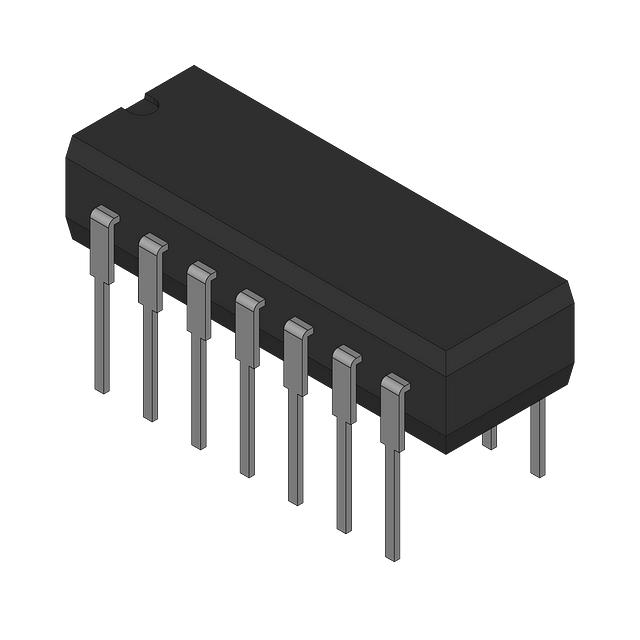
SN54LS266J

Why Choose Us?
Professional Platform
B2B & B2C purchasingDelivery at full speed
1-2 days deliveryWide variety
Original manufacturers365 days guarantee
Responsible quality
.png)


Tech Specifications
SN54LS266J Description
The SN54LS266J is a high-speed quad bilateral switch manufactured by Texas Instruments. This device is designed to provide high-speed switching and gating capabilities in a variety of applications.
Description:
The SN54LS266J is a 16-pin integrated circuit (IC) that contains four bilateral switches. Each switch is capable of handling high-speed signals with a propagation delay of only 15 ns. The device is designed to operate over a wide range of supply voltages, from 4.75V to 5.25V, and can handle input signals with a voltage as low as 0.3V.
Features:
Some of the key features of the SN54LS266J include:
- High-speed switching: The device is designed to handle high-speed signals with a propagation delay of only 15 ns.
- Wide operating voltage range: The device can operate over a wide range of supply voltages, from 4.75V to 5.25V.
- Low input voltage requirements: The device can handle input signals with a voltage as low as 0.3V.
- Quad bilateral switches: The device contains four bilateral switches, providing flexibility in switching and gating applications.
- TTL and CMOS compatible: The device is compatible with both TTL and CMOS logic families, making it suitable for a wide range of applications.
Applications:
The SN54LS266J is commonly used in a variety of applications, including:
- Digital signal processing: The device can be used to switch and gate high-speed digital signals in digital signal processing applications.
- Data acquisition systems: The device can be used to switch and gate signals in data acquisition systems, such as in medical or industrial equipment.
- Telecommunications: The device can be used in telecommunications equipment to switch and gate high-speed signals.
- Test and measurement equipment: The device can be used in test and measurement equipment to switch and gate signals during testing and measurement processes.
- Computer systems: The device can be used in computer systems to switch and gate signals between various components.
Overall, the SN54LS266J is a versatile and high-speed switching and gating device that is suitable for a wide range of applications requiring high-speed signal handling.
FAQ
| Quantity | Unit Price | Ext. Price |
|---|---|---|
| 18+ | $14.68720 | $264.37 |
Not available to buy online? Want the lower wholesale price? Please Send RFQ to get best price, we will respond immediately


.png?x-oss-process=image/format,webp/resize,h_32)


