
 German
 Japanese
 Portuguese
 Korea
Korea
 Mexico
 Dutch
Dutch


Texas Instruments
SN54LS283J

Why Choose Us?
Professional Platform
B2B & B2C purchasingDelivery at full speed
1-2 days deliveryWide variety
Original manufacturers365 days guarantee
Responsible quality
.png)


Tech Specifications
SN54LS283J Description
The SN54LS283J is a quad 2-input NAND gate integrated circuit (IC) manufactured by Texas Instruments. It is a part of the 74LS series, which are low-power Schottky logic devices. Here's a brief description, features, and applications of the SN54LS283J:
Description:
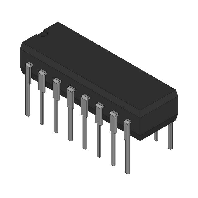
The SN54LS283J is a 14-pin DIP (Dual In-Line Package) or SOIC (Small Outline Integrated Circuit) package containing four independent 2-input NAND gates. NAND gates are fundamental building blocks in digital electronics, and they perform a logical AND operation followed by a NOT operation. The output of a NAND gate is LOW only when both inputs are HIGH.
Features:
- Quad 2-input NAND gate configuration.
- 74LS series: Low-power Schottky logic family.
- 14-pin DIP or SOIC package options.
- Wide operating voltage range: 2V to 6V.
- High noise immunity.
- Suitable for TTL (Transistor-Transistor Logic) and CMOS (Complementary Metal-Oxide-Semiconductor) compatibility.
- Low power consumption.
- Fast switching times.
Applications:
- Digital logic circuits: The SN54LS283J can be used to build various digital logic circuits, such as decoders, encoders, and multiplexers, by combining NAND gates.
- Logic gate experiments: It is suitable for educational purposes and experimenting with basic digital logic concepts.
- Electronics projects: The SN54LS283J can be used in various electronic projects that require logic operations, such as control systems, signal processing, and data storage.
- Microcontroller interfacing: It can be used to interface microcontrollers with external circuits, providing additional logic functions.
- DIY electronics: Hobbyists and DIY enthusiasts can use the SN54LS283J to create custom electronic circuits and systems.
In summary, the SN54LS283J is a versatile quad 2-input NAND gate IC from Texas Instruments that offers low power consumption, high noise immunity, and compatibility with both TTL and CMOS devices. It is suitable for a wide range of applications, including digital logic design, educational purposes, and various electronic projects.
FAQ
| Quantity | Unit Price | Ext. Price |
|---|---|---|
| 27+ | $9.98800 | $269.68 |
Not available to buy online? Want the lower wholesale price? Please Send RFQ to get best price, we will respond immediately


.png?x-oss-process=image/format,webp/resize,h_32)


