

Texas Instruments
SN74ABT541BN
Buffers, Drivers, Receivers, Transceivers

Not available to buy online? Want the lower wholesale price? Please Send RFQ to get best price, we will respond immediately


.png?x-oss-process=image/format,webp/resize,p_30)


SN74ABT541BN Description
SN74ABT541BN Description
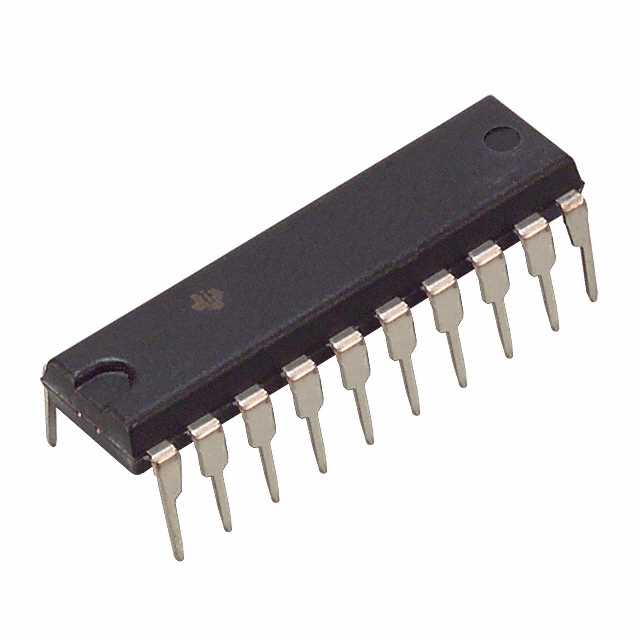
The SN74ABT541BN is a high-performance logic IC chip designed by Texas Instruments, part of the 74ABT series. This chip is a non-inverting buffer with 8 bits per element, making it highly suitable for applications requiring efficient data transmission and signal conditioning. The SN74ABT541BN operates within a supply voltage range of 4.5V to 5.5V, ensuring compatibility with a wide range of digital systems. It is packaged in a through-hole 20DIP format, which facilitates easy integration into various circuit boards and systems.
SN74ABT541BN Features
- High Current Capability: The SN74ABT541BN offers an output current of 32mA for high levels and 64mA for low levels, making it capable of driving multiple loads efficiently.
- Wide Operating Voltage Range: With a supply voltage range of 4.5V to 5.5V, this IC is versatile and can be used in systems with varying power supply requirements.
- Non-Inverting Buffer: The non-inverting nature of the buffer ensures that the output signal maintains the same logical state as the input, simplifying circuit design.
- Through-Hole Mounting: The through-hole mounting type provides robust mechanical stability and is ideal for applications requiring high reliability and long-term durability.
- Compliance and Standards: The SN74ABT541BN is REACH unaffected and RoHS3 compliant, ensuring it meets environmental and safety standards. It also carries an ECCN of EAR99, indicating its classification under export regulations.
- Packaging: Available in a tube package, the SN74ABT541BN is protected during shipping and storage, reducing the risk of damage.
SN74ABT541BN Applications
The SN74ABT541BN is ideal for a variety of applications due to its robust performance and compatibility with different voltage levels. Some specific use cases include:
- Data Transmission: The high current capability and non-inverting nature make it suitable for buffering data lines in communication systems.
- Signal Conditioning: It can be used to condition signals in digital systems, ensuring that the output signal is clean and stable.
- Industrial Control Systems: The through-hole mounting and wide operating voltage range make it suitable for industrial applications where reliability and durability are critical.
- Consumer Electronics: The SN74ABT541BN can be used in consumer electronics for driving multiple loads and ensuring signal integrity.
Conclusion of SN74ABT541BN
The SN74ABT541BN from Texas Instruments is a versatile and reliable logic IC chip that offers a range of benefits for various applications. Its high current capability, wide operating voltage range, and non-inverting buffer design make it a valuable component in digital systems. The through-hole mounting and compliance with environmental and safety standards further enhance its appeal. Whether used in data transmission, signal conditioning, or industrial control systems, the SN74ABT541BN provides a robust and efficient solution for engineers and designers in the electronics industry.
Tech Specifications
SN74ABT541BN Documents
Download datasheets and manufacturer documentation for SN74ABT541BN
Mechanical Outline Drawing Add Cu as Alternative Bond Wire Metal for Select Devices (PDF) Product Change Notification (PDF) Logic Guide (Rev. AB) Advanced Bus Interface Logic Selection Guide SN74ABT541B Behavioral SPICE Model Related Parts


Shopping Guide


.png?x-oss-process=image/format,webp/resize,h_32)


©2025 ERSA Electronics Corporation.