
Texas Instruments
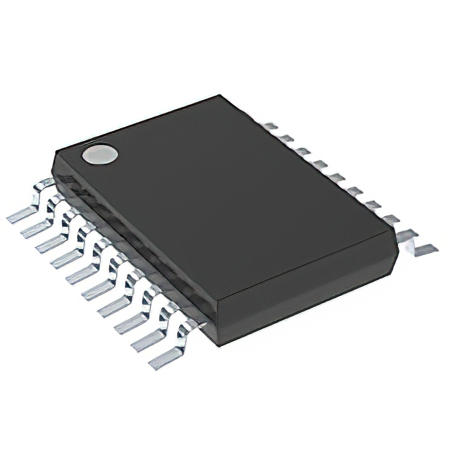
SN74AC244PWR
Buffers, Drivers, Receivers, Transceivers


.png?x-oss-process=image/format,webp/resize,p_30)


SN74AC244PWR Description
The Texas Instruments SN74AC244PWR is a high-performance, 8-bit, parallel-in, parallel-out (PISO) shift register that is designed for use in a wide range of applications. Here is a brief description of the device, its features, and potential applications:
Description:
The SN74AC244PWR is a member of the 74ACxx family of advanced CMOS logic devices. It is an 8-bit shift register that allows for parallel input and parallel output of data. The device is designed to operate with a wide supply voltage range and offers high noise immunity, making it suitable for use in various electronic systems.
Features:
- 8-bit Shift Register: The device can store and shift up to 8 bits of data in parallel.
- Parallel Input and Output: It allows for simultaneous data input and output, which can be useful for high-speed data processing.
- Wide Supply Voltage Range: It operates with a supply voltage range of 2V to 6V, making it suitable for a variety of power supply configurations.
- High Noise Immunity: The device is designed to resist noise, ensuring reliable operation in noisy environments.
- Low Power Consumption: It is designed to consume low power, making it suitable for battery-powered or energy-sensitive applications.
- High-Speed Operation: The device is capable of high-speed operation, with typical propagation delays of around 3.5 ns (maximum) at a supply voltage of 5V.
- Temperature Range: It can operate over a wide temperature range of -40°C to +85°C, making it suitable for both commercial and industrial applications.
Applications:
- Data Buffering: In systems where data needs to be temporarily stored and then transferred, the SN74AC244PWR can be used as a buffer.
- Serial-to-Parallel Conversion: It can be used to convert serial data into parallel data, which can be beneficial in systems that require parallel data processing.
- Parallel-to-Serial Conversion: Although the device is primarily a PISO shift register, it can also be used in conjunction with other logic to perform parallel-to-serial conversion.
- High-Speed Data Communication: Due to its high-speed operation, it can be used in applications that require fast data transfer, such as in digital communication systems.
- Digital Signal Processing: It can be used in digital signal processing applications where data manipulation and storage are required.
- Automotive Electronics: Given its wide temperature range and noise immunity, it can be used in automotive electronics for reliable data handling.
- Industrial Control Systems: It can be used in industrial control systems where high noise immunity and reliable operation are critical.
When using the SN74AC244PWR, it is important to consult the datasheet for detailed information on pin configurations, power consumption, timing specifications, and other technical details to ensure proper integration into a specific application.
Tech Specifications
SN74AC244PWR Documents
Download datasheets and manufacturer documentation for SN74AC244PWR
 Mechanical Outline Drawing
  Product Change Notification 2024-10-23 (PDF) Qualification of Mold Compound for Select Devices using TSSOP package (PDF) Product Change Notification 2024-10-07 (PDF) Product Change Notification (PDF)
  SN74AC244PWR Symbol & Footprint by SnapMagic
  Logic Guide (Rev. AB)
  Simultaneous-Switching Performance of TI Logic Devices (Rev. B)
  SN74AC244 Behavioral SPICE Model
 Shopping Guide


.png?x-oss-process=image/format,webp/resize,h_32)


