
 German
 Japanese
 Portuguese
 Korea
Korea
 Mexico
 Dutch
Dutch


Texas Instruments
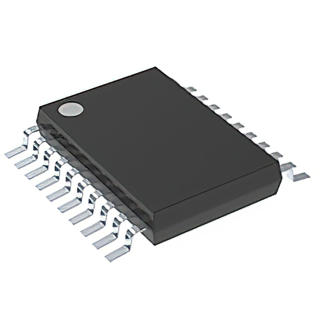
SN74ACT244IPWRQ1

Why Choose Us?
Professional Platform
B2B & B2C purchasingDelivery at full speed
1-2 days deliveryWide variety
Original manufacturers365 days guarantee
Responsible quality
.png)


Tech Specifications
SN74ACT244IPWRQ1 Description
The Texas Instruments SN74ACT244IPWRQ1 is a high-performance, 8-input, multiplexer (MUX) that is designed to provide high-speed signal routing in a variety of applications.
Description:
The SN74ACT244IPWRQ1 is a member of the 74ACTxx family of CMOS logic devices. It is a 8-input multiplexer that allows one of eight input signals to be selected and routed to a single output. The device is available in a 20-pin QFN package.
Features:
- 8-input multiplexer
- 3 select inputs (A0, A1, A2) to choose the active input
- High-speed performance: propagation delay as low as 2.7 ns
- Low power consumption: 2.4 mA maximum at 5 V
- 3-state outputs for easy cascading
- Wide operating voltage range: 2.0 V to 6.0 V
- Available in a 20-pin QFN package
Applications:
The SN74ACT244IPWRQ1 is well-suited for a variety of applications that require high-speed signal routing, including:
- Digital signal processing (DSP)
- Video processing
- Telecommunications
- Data acquisition and control systems
- Audio processing
- Industrial control systems
The device's high-speed performance and low power consumption make it an excellent choice for battery-powered applications, while its 3-state outputs allow for easy cascading to support larger signal routing requirements. Its wide operating voltage range also makes it suitable for use in a variety of different systems and environments.
FAQ
| Quantity | Unit Price | Ext. Price |
|---|---|---|
| 1+ | $0.50057 | $0.50 |
| 10+ | $0.48685 | $4.87 |
| 30+ | $0.47828 | $14.35 |
| 100+ | $0.46972 | $46.97 |
Not available to buy online? Want the lower wholesale price? Please Send RFQ to get best price, we will respond immediately


.png?x-oss-process=image/format,webp/resize,h_32)


