
Texas Instruments
SN74AHC1G08QDBVRQ1
Gates and Inverters


.png?x-oss-process=image/format,webp/resize,p_30)


SN74AHC1G08QDBVRQ1 Description
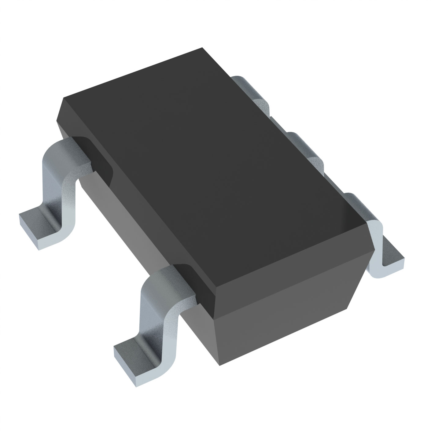
The SN74AHC1G08QDBVRQ1 is a high-speed Si-gate CMOS device manufactured by Texas Instruments. It is a quad 2-input AND gate, which means it has four independent AND gates in a single package. The device is designed to meet the requirements of high-speed applications and is suitable for both digital and analog signal processing.
Description:
The SN74AHC1G08QDBVRQ1 is a member of the 74AHC/AHCT family of CMOS devices. It is a quad 2-input AND gate, which means it has four independent AND gates in a single package. Each gate has two input signals and one output signal. The output is true (high) only when both input signals are true (high). The device is available in a QFN (Quad Flat No-leads) package with a thermal pad for better heat dissipation.
Features:
- High-speed operation: The device is designed for high-speed applications and can operate at a frequency of up to 340 MHz.
- Low power consumption: The device has a low power consumption of 1.4 mA maximum, making it suitable for battery-powered applications.
- Wide operating voltage range: The device can operate over a wide voltage range of 1.65V to 5.5V, making it suitable for a variety of applications.
- High noise immunity: The device has high noise immunity, making it suitable for use in noisy environments.
- RoHS compliant: The device is compliant with the Restriction of Hazardous Substances (RoHS) directive, which restricts the use of hazardous materials in electronic products.
Applications:
The SN74AHC1G08QDBVRQ1 is suitable for a wide range of applications, including:
- Digital signal processing: The device can be used in digital signal processing applications where high-speed operation and low power consumption are required.
- Logic gates: The device can be used as a building block for constructing more complex logic gates and circuits.
- Analog signal processing: The device can be used in analog signal processing applications where high noise immunity is required.
- Battery-powered applications: The low power consumption of the device makes it suitable for use in battery-powered applications.
- Industrial control systems: The device can be used in industrial control systems where high-speed operation and wide operating voltage range are required.
In summary, the SN74AHC1G08QDBVRQ1 is a high-speed, low-power, quad 2-input AND gate that is suitable for a wide range of applications, including digital signal processing, logic gates, analog signal processing, battery-powered applications, and industrial control systems. Its features, such as high noise immunity and RoHS compliance, make it a reliable choice for various applications.
Tech Specifications
SN74AHC1G08QDBVRQ1 Documents
Download datasheets and manufacturer documentation for SN74AHC1G08QDBVRQ1
 SN74AHC1G08-Q1 Logic Guide
  SN74AHC1G08-Q1 Logic Guide
  Mult Dev Assembly Wafer Site/Design 21/Dec/2023
 Shopping Guide


.png?x-oss-process=image/format,webp/resize,h_32)


