
 German
 Japanese
 Portuguese
 Korea
Korea
 Mexico
 Dutch
Dutch


Texas Instruments
SN74AHC1G126DCKR

Why Choose Us?
Professional Platform
B2B & B2C purchasingDelivery at full speed
1-2 days deliveryWide variety
Original manufacturers365 days guarantee
Responsible quality
.png)


Tech Specifications
SN74AHC1G126DCKR Description
The Texas Instruments SN74AHC1G126DCKR is a high-speed quad 2-input OR gate. It is part of the 74AHC/AHCT1G series of logic gates, which are designed to provide high performance and low power consumption in a small package.
Description:
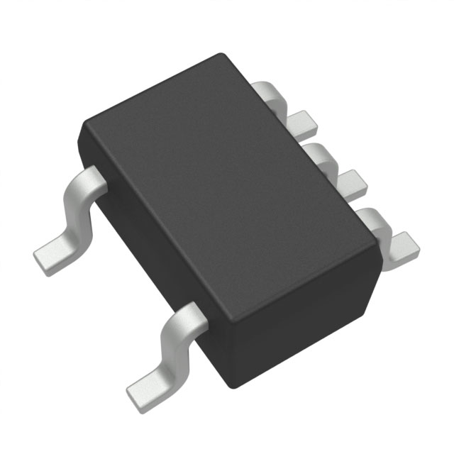
The SN74AHC1G126DCKR is a quad 2-input OR gate, which means it has four independent OR gate functions in a single package. The OR gate is a fundamental building block of digital logic circuits, and it produces a high output (1) when at least one of its inputs is high (1). The SN74AHC1G126DCKR is available in a 6-pin SOT-363 package.
Features:
- High-speed performance: The SN74AHC1G126DCKR has a propagation delay of only 3.5 ns, making it suitable for high-speed applications.
- Low power consumption: The device has a low power consumption of only 1.8 mW per gate, which makes it ideal for battery-powered or energy-sensitive applications.
- Wide operating voltage range: The SN74AHC1G126DCKR can operate over a wide voltage range of 1.65V to 5.5V, making it suitable for a variety of applications.
- High noise immunity: The device has high noise immunity, with a typical noise margin of 0.9V.
Applications:
The SN74AHC1G126DCKR can be used in a variety of digital logic applications, including:
- Digital logic circuits: The SN74AHC1G126DCKR can be used to build complex digital logic circuits, such as adders, subtractors, and decoders.
- Signal amplification: The OR gate can be used to amplify signals by combining multiple input signals into a single output signal.
- Logic conversion: The SN74AHC1G126DCKR can be used to convert logic signals from one format to another, such as from open-drain to totem-pole output.
- Glitch suppression: The OR gate can be used to suppress glitches in digital circuits by combining multiple input signals that may have different rise and fall times.
Overall, the Texas Instruments SN74AHC1G126DCKR is a versatile and high-performance quad 2-input OR gate that is suitable for a wide range of digital logic applications. Its high speed, low power consumption, and wide operating voltage range make it an ideal choice for designers looking for a reliable and efficient logic gate solution.
FAQ
| Quantity | Unit Price | Ext. Price |
|---|---|---|
| 10+ | $0.08855 | $0.89 |
| 100+ | $0.06979 | $6.98 |
| 300+ | $0.06041 | $18.12 |
| 3000+ | $0.04817 | $144.51 |
| 6000+ | $0.04255 | $255.30 |
Not available to buy online? Want the lower wholesale price? Please Send RFQ to get best price, we will respond immediately


.png?x-oss-process=image/format,webp/resize,h_32)


