
Texas Instruments
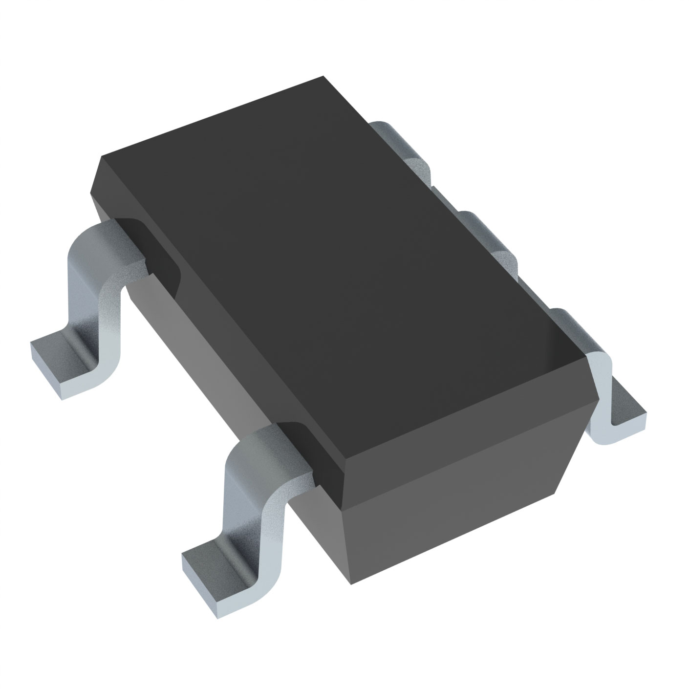
SN74AHC1G14DBVR
Gates and Inverters


- 10+
- $0.05978
- $0.6
- 100+
- $0.04834
- $4.83
- 300+
- $0.04261
- $12.78
- 3000+
- $0.03615
- $108.45
- 6000+
- $0.03272
- $196.32
- 9000+
- $0.03100
- $279

.png?x-oss-process=image/format,webp/resize,p_30)


SN74AHC1G14DBVR Description
The SN74AHC1G14DBVR is a high-speed Si-gate CMOS device from Texas Instruments. It is a dual bus buffer with three-state outputs that is designed to provide high performance in a wide range of applications. Here is a detailed description of the model, its features, and potential applications:
Description:
The SN74AHC1G14DBVR is a member of the 74AHC/AHCT1G series of devices, which are designed to offer high-speed operation with low power consumption. This particular device is a dual bus buffer with three-state outputs, meaning it can be used to control the flow of data between different parts of a system, and it can also be put into a high-impedance state (three-state) when not in use.
Features:
-
High-Speed Operation: The device is designed for high-speed operation, making it suitable for use in systems that require fast data transfer rates.
-
Low Power Consumption: Despite its high-speed capabilities, the SN74AHC1G14DBVR is designed to consume low power, which is beneficial for battery-powered or energy-sensitive applications.
-
Three-State Outputs: The three-state outputs allow the device to be put into a high-impedance state when not in use, which can help to reduce power consumption and prevent conflicts in a system with multiple drivers.
-
Si-gate CMOS Technology: The use of Si-gate CMOS technology provides a high level of integration and performance, making the device suitable for a wide range of applications.
-
Dual Bus Buffer: The device can be used to buffer two separate data buses, allowing for efficient data transfer between different parts of a system.
Applications:
-
Data Buffering: The device can be used to buffer data buses in a variety of systems, including computers, servers, and other data processing equipment.
-
Communications Systems: The high-speed operation and three-state outputs make the SN74AHC1G14DBVR suitable for use in communication systems, where data must be transferred quickly and accurately.
-
Automotive Systems: The low power consumption and high-speed operation of the device make it suitable for use in automotive systems, where reliability and efficiency are critical.
-
Industrial Control Systems: The device can be used in industrial control systems to buffer data between different components, helping to ensure efficient and reliable operation.
-
Embedded Systems: The SN74AHC1G14DBVR can be used in embedded systems to control the flow of data between different parts of the system, improving overall performance and reliability.
In summary, the SN74AHC1G14DBVR is a versatile and high-performance device that can be used in a wide range of applications where high-speed data transfer and efficient power consumption are important. Its three-state outputs and dual bus buffering capabilities make it particularly useful in complex systems where multiple data buses need to be controlled.
Tech Specifications
SN74AHC1G14DBVR Documents
Download datasheets and manufacturer documentation for SN74AHC1G14DBVR
 Mult Dev A/T Chgs 30/Aug/2023
  SN74AHC1G14
  Mult Dev Design/Assembly Site 21/Dec/2023
  SN74AHC1G14
 Shopping Guide


.png?x-oss-process=image/format,webp/resize,h_32)


