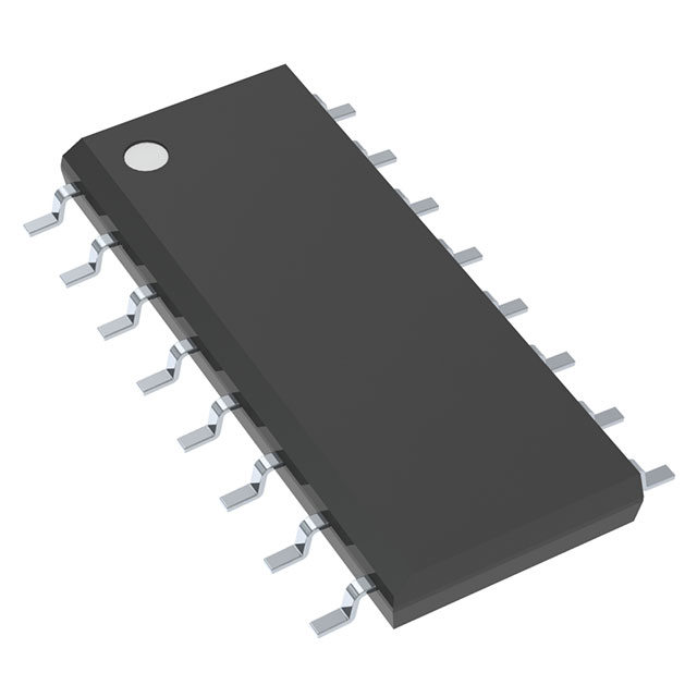
Texas Instruments_SN74AHC595DR

Texas Instruments
SN74AHC595DR  
Shift Registers

Texas Instruments
SN74AHC595DR
712-SN74AHC595DR
Ersa
Texas Instruments-SN74AHC595DR-datasheets-1909588.pdf
IC SHIFT REGISTER 8BIT 16-SOIC
In Stock : 2822

Not available to buy online? Want the lower wholesale price? Please Send RFQ to get best price, we will respond immediately

QUICK RFQ
ADD TO RFQ LIST
ersa FreeSample ersa flow
  • Quantity
  • Unit Price
  • Ext. Price
    • 5+
    • $0.34798
    • $1.74
    • 50+
    • $0.28419
    • $14.21
    • 150+
    • $0.25685
    • $38.53
    ADD TO CART
    QUICK ORDER
    $0.00000    $0.00
    ISO9001
    Quality Policy
    ISO45001
    ISO14001

    SN74AHC595DR Description

    The SN74AHC595DR is a high-speed 8-bit shift register manufactured by Texas Instruments. It is a part of the 74AHC/HCT series of logic devices, which are designed to operate with low voltage and low power consumption while providing high performance.

    Description:

    The SN74AHC595DR is a serial-in, parallel-out shift register that can store and transmit 8 bits of data at a time. It has a serial input (DS) for shifting data into the register, a parallel input (D0 to D7) for loading data directly, and a parallel output (Q0 to Q7) for retrieving the stored data. The device also features a storage register and a shift register, allowing it to store and shift data simultaneously.

    Features:

    1. 8-bit serial-in, parallel-out shift register
    2. 3-state outputs for flexible bus applications
    3. Compatible with TTL and CMOS logic levels
    4. Wide operating voltage range (2V to 6V)
    5. Low power consumption (typical 2.2mA at 5V)
    6. High-speed operation (typical 7.5ns propagation delay at 5V)
    7. Active-low serial and parallel load control inputs (SH_CP and ST_CP)
    8. Active-low output enable control input (OE)
    9. Active-low master reset input (MR)

    Applications:

    1. LED display scanning and control in multiplexed LED displays
    2. Data storage and transmission in serial communication systems
    3. Shift register applications in digital signal processing
    4. Data buffering and level conversion in digital circuits
    5. Expanding the number of parallel outputs from a microcontroller or processor
    6. Driving relays, solenoids, or other high-current loads
    7. Synchronization of data in digital systems

    The SN74AHC595DR is a versatile and efficient shift register that can be used in a wide range of applications where data storage, transmission, and manipulation are required. Its compatibility with both TTL and CMOS logic levels, low power consumption, and high-speed operation make it suitable for various digital designs.

    Tech Specifications

    Unit Weight
    Configuration
    Maximum Propagation Delay Time @ Maximum CL (ns)
    Parallel Enable Input
    Product
    PPAP
    Supply voltage (min) (V)
    Product Status
    Number of Stages
    Automotive
    RoHS
    Supplier Package
    Package / Case
    Absolute Propagation Delay Time (ns)
    Voltage - Supply
    Logic Function
    REACH Status
    Triggering Type
    Output type
    Number of Element Outputs
    Maximum Operating Supply Voltage (V)
    Number of Elements
    Number of Bits
    EU RoHS
    Carrier
    Clock frequency (MHz)
    Moisture Sensitivity Level (MSL)
    Operating Temperature
    Operating temperature range (°C)
    Logic Type
    ECCN
    MSL rating / Peak reflow
    Mounting Type
    Standard Package Name
    Terminal Count Output
    Pin Count
    Operation Mode
    Mounting
    Lead Shape
    Typical Operating Supply Voltage (V)
    HTSUS
    Package
    Pins
    IOH (max) (mA)
    USHTS
    Propagation Delay Time
    PCB changed
    Bits (#)
    Output Type
    HTS
    Number of Elements per Chip
    Rating
    ECCN (US)
    Supply current (max) (µA)
    Supplier Device Package
    Direction Type
    Supply Voltage - Min
    Minimum Operating Temperature (°C)
    Maximum Operating Temperature (°C)
    Function
    Process Technology
    Propagation Delay Test Condition (pF)
    Package Height
    Number of Count Input Enables
    Mfr
    Supply voltage (max) (V)
    Maximum Operating Temperature
    Features
    Number of Selection Inputs per Element
    Supply Voltage - Max
    Width
    RoHS Status
    Mounting Style
    Counting Sequence
    Technology family
    Number of Bits per Element
    Number of Input Lines
    Number of Element Inputs
    Package Length
    Minimum Operating Temperature
    REACH
    Series
    Input type
    Number of Output Lines
    IOL (max) (mA)
    Operating Supply Voltage
    Part Status
    Lead finish / Ball material
    Logic Family
    Package Width
    Number of Circuits
    Base Product Number
    Minimum Operating Supply Voltage (V)

    SN74AHC595DR Documents

    Download datasheets and manufacturer documentation for SN74AHC595DR

    Ersa Mechanical Outline Drawing      
    Ersa Product Change Notification_2024_10_25 (PDF)       Product Change Notification 2024-05-31 (PDF)       Product Change Notification (PDF)      
    Ersa SN74AHC595DR Symbol & Footprint by SnapMagic      
    Ersa Logic Guide (Rev. AB)       Little Logic Guide 2018 (Rev. G)      

    Shopping Guide

    Payment Methods
    Payment Methods include Prepayment TT (bank transfer), Western Union, and PayPal. Customers are responsible for shipping costs, bank charges, customs duties and taxes.
    Shipping Rate
    Shipments are made once a day around 5pm, excluding Sundays. Once shipped, the estimated delivery time is usually 5-7 business days, depending on the courier you choose.
    Delivery Methods
    Provide DHL, FedEx, UPS, EMS, SF Express and Registered Airmail International Delivery Service