
Texas Instruments
SN74AHCT1G125DBVT
Buffers, Drivers, Receivers, Transceivers


.png?x-oss-process=image/format,webp/resize,p_30)


SN74AHCT1G125DBVT Description
SN74AHCT1G125DBVT Description
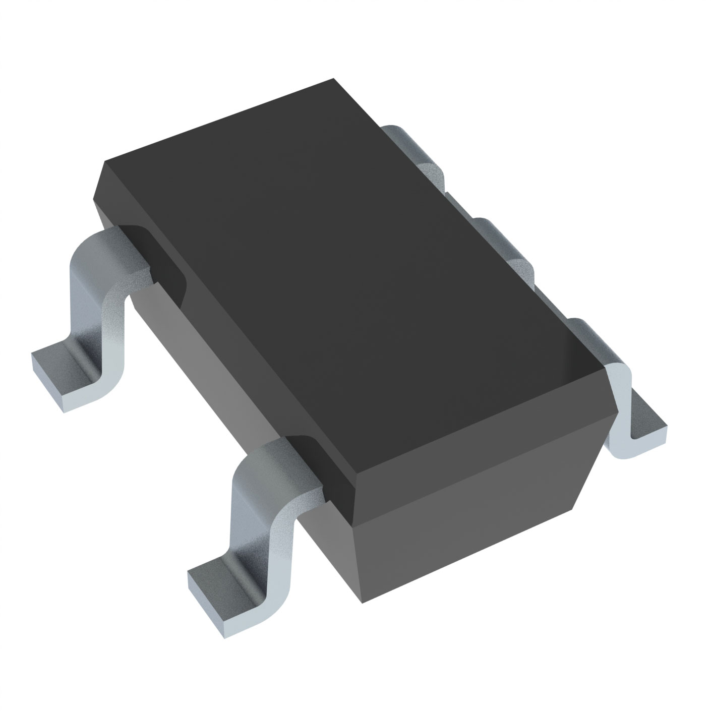
The SN74AHCT1G125DBVT from Texas Instruments is a high-performance, single-bit non-inverting buffer/driver with 3-state output, designed for 4.5V to 5.5V voltage supply systems. Packaged in a compact SOT23-5 form factor, this device is ideal for space-constrained applications. It belongs to the 74AHCT series, known for its robust CMOS/TTL compatibility, making it suitable for interfacing between low-voltage and higher-voltage systems. With 8mA output current (both high and low), it ensures strong signal integrity in noisy environments. The device is RoHS3 compliant, REACH unaffected, and features a Moisture Sensitivity Level (MSL) 1 rating, ensuring reliability in industrial and consumer applications.
SN74AHCT1G125DBVT Features
- Single-Bit Non-Inverting Buffer: Provides signal isolation and drive capability without logic inversion.
- 3-State Output: Allows multiple devices to share a common bus without interference.
- Wide Voltage Range (4.5V–5.5V): Compatible with TTL levels, ensuring seamless integration in mixed-voltage systems.
- High Output Current (8mA): Capable of driving capacitive loads and long traces with minimal signal degradation.
- Low Power Consumption: Optimized for battery-operated and power-sensitive designs.
- Robust Packaging: SOT23-5 tape-and-reel (TR) packaging enables automated assembly and reduces board space.
- Industry-Standard Compliance: RoHS3, REACH, and MSL1 certified for global deployment.
SN74AHCT1G125DBVT Applications
- Bus Buffering/Isolation: Ideal for I²C, SPI, and other shared-bus systems requiring signal conditioning.
- Level Shifting: Bridges 3.3V and 5V logic domains in mixed-voltage designs.
- Portable Electronics: Used in smartphones, tablets, and wearables due to its low power and small footprint.
- Industrial Control Systems: Provides noise immunity in PLCs, motor drivers, and sensor interfaces.
- Automotive Electronics: Suitable for infotainment and control modules where reliability is critical.
Conclusion of SN74AHCT1G125DBVT
The SN74AHCT1G125DBVT combines high drive strength, TTL compatibility, and compact packaging, making it a versatile solution for buffering, level shifting, and signal isolation. Its low power consumption and robust ESD protection make it ideal for both consumer and industrial applications. For engineers seeking a reliable, space-efficient buffer with 3-state control, this device stands out among similar models for its performance, compliance, and ease of integration.
Tech Specifications
SN74AHCT1G125DBVT Documents
Download datasheets and manufacturer documentation for SN74AHCT1G125DBVT
 Product Discontinuation Notification (PDF)
  Mechanical Outline Drawing
  Add Cu as Alternative Wire Base Metal for Selected Device(s) on QFN, QFP and SOT-23 packages (PDF) Qualification of Cu as Alternative Wire Base Metal for Selected Device(s) (PDF) Product Change Notification (PDF)
  SN74AHCT1G125DBVT Symbol & Footprint by SnapMagic
  Logic Guide (Rev. AB) Little Logic Guide 2018 (Rev. G)
  SN74AHCT1G125 Behavioral SPICE Model HSPICE Model for SN74AHCT1G125 SN74AHCT1G125 PSpice Model
 Shopping Guide


.png?x-oss-process=image/format,webp/resize,h_32)


