
Texas Instruments
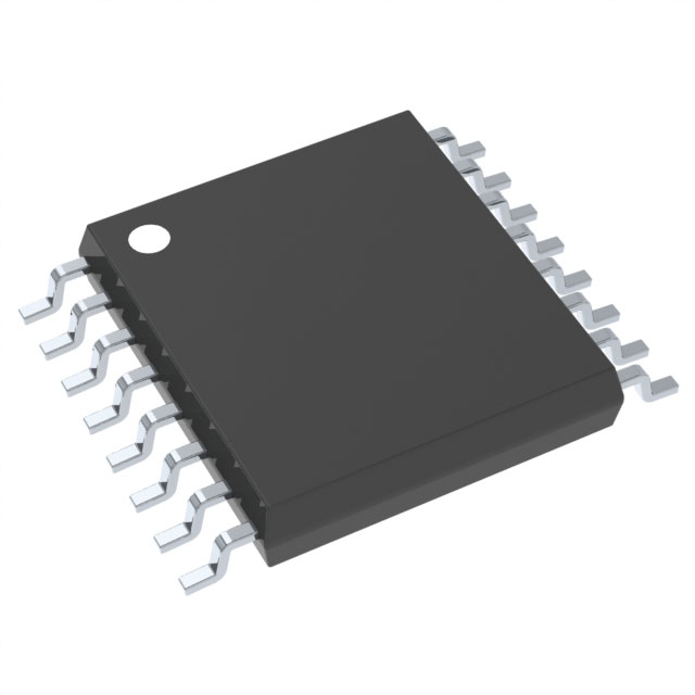
SN74AHCT367PWR
Buffers, Drivers, Receivers, Transceivers


- 1+
- $0.41234
- $0.41
- 10+
- $0.40241
- $4.02
- 30+
- $0.39744
- $11.92

.png?x-oss-process=image/format,webp/resize,p_30)


SN74AHCT367PWR Description
The SN74AHCT367PWR is a high-performance quad 2-input multiplexer (MUX) manufactured by Texas Instruments. It is a member of the 74AHC/AHCT family of logic devices, which are designed for high-speed operation and low power consumption. The device is available in a 20-pin package.
Description:
The SN74AHCT367PWR is a quad 2-input multiplexer that allows one of four input signals to be selected and passed through to the output based on the state of the select input lines. The device has two select inputs (S0 and S1) that determine which of the four input signals is passed through to the output. The device also features a true single-pole, quad-throw (TSPT) configuration, which means that the output is connected to one of the four inputs at any given time.
Features:
- High-speed operation: The SN74AHCT367PWR is designed for high-speed operation, with a propagation delay of only 3.6 ns (typical) at a supply voltage of 5V.
- Low power consumption: The device has a low power consumption of only 2.2 mW per gate at a supply voltage of 5V.
- Wide supply voltage range: The SN74AHCT367PWR can operate over a wide supply voltage range of 2V to 6V.
- TTL and CMOS compatible: The device is compatible with both TTL and CMOS logic families, making it suitable for use in a wide range of applications.
- True single-pole, quad-throw (TSPT) configuration: The device has a TSPT configuration, which allows for efficient signal routing and selection.
Applications:
The SN74AHCT367PWR can be used in a variety of applications where signal routing and selection are required. Some common applications include:
- Digital signal processing: The device can be used to route digital signals in digital signal processing (DSP) systems.
- Telecommunications: The SN74AHCT367PWR can be used in telecommunications systems for signal routing and selection.
- Data multiplexing: The device can be used to multiplex multiple data signals into a single signal for transmission over a shared communication channel.
- Logic control systems: The SN74AHCT367PWR can be used in logic control systems to route control signals based on the state of the select inputs.
- Test and measurement equipment: The device can be used in test and measurement equipment for signal routing and selection during testing and debugging.
In summary, the SN74AHCT367PWR is a high-performance quad 2-input multiplexer that offers high-speed operation, low power consumption, and compatibility with both TTL and CMOS logic families. It is suitable for a wide range of applications where signal routing and selection are required.
Tech Specifications
SN74AHCT367PWR Documents
Download datasheets and manufacturer documentation for SN74AHCT367PWR
 SN54/74AHCT367
  SN54/74AHCT367
 Shopping Guide


.png?x-oss-process=image/format,webp/resize,h_32)


