
 German
 Japanese
 Portuguese
 Korea
Korea
 Mexico
 Dutch
Dutch


Texas Instruments
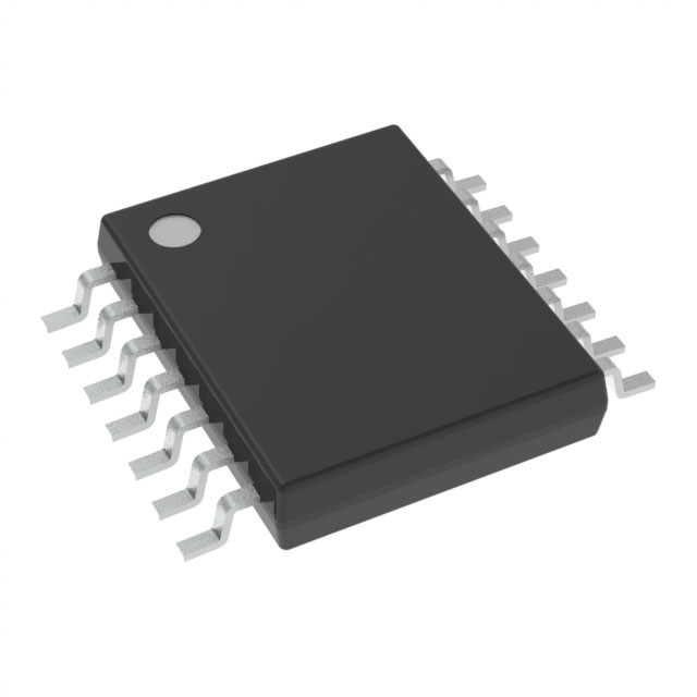
SN74ALVC125PW

Why Choose Us?
Professional Platform
B2B & B2C purchasingDelivery at full speed
1-2 days deliveryWide variety
Original manufacturers365 days guarantee
Responsible quality
.png)


Tech Specifications
SN74ALVC125PW Description
SN74ALVC125PW Description
The SN74ALVC125PW from Texas Instruments is a high-performance, quad-channel non-inverting buffer/line driver designed for 1.65V to 3.6V voltage operation. Packaged in a 14-pin TSSOP (Thin Shrink Small Outline Package), this device is optimized for surface-mount applications and is part of the 74ALVC series, known for its low-voltage capabilities and robust signal integrity. With 4 independent buffers, each featuring tri-state outputs, it enables efficient bus interfacing and signal isolation. The device is RoHS3 compliant, REACH unaffected, and rated for MSL 1 (Unlimited) moisture sensitivity, making it suitable for industrial and commercial environments.
SN74ALVC125PW Features
- Wide Voltage Range: Operates from 1.65V to 3.6V, ideal for mixed-voltage systems.
- High Drive Strength: Delivers ±24mA output current, ensuring reliable signal transmission in noisy environments.
- Low Power Consumption: Optimized for power-sensitive applications with minimal static power dissipation.
- Tri-State Outputs: Allows multiple devices to share a common bus without interference.
- Fast Propagation Delay: Ensures high-speed signal processing, critical for timing-sensitive designs.
- Robust Packaging: 14-TSSOP offers compact footprint and thermal efficiency for dense PCB layouts.
- Environmental Compliance: ROHS3 and REACH compliant, meeting global environmental standards.
SN74ALVC125PW Applications
- Bus Interface Circuits: Ideal for I²C, SPI, and UART communication systems requiring signal buffering.
- Portable Electronics: Suited for battery-powered devices (e.g., smartphones, IoT sensors) due to low-voltage operation.
- Industrial Control Systems: Used in PLC modules, motor drivers, and other noise-prone environments.
- Automotive Electronics: Supports CAN/LIN bus interfaces in vehicle networking applications.
- FPGA/Processor Interfacing: Provides level shifting and signal isolation in embedded systems.
Conclusion of SN74ALVC125PW
The SN74ALVC125PW stands out as a versatile, high-performance buffer solution for modern low-voltage digital systems. Its wide operating range, high drive capability, and tri-state functionality make it superior to conventional buffers in mixed-signal environments. Whether for portable, industrial, or automotive applications, this device ensures reliable signal integrity while adhering to stringent environmental and quality standards. Its compact TSSOP package further enhances its suitability for space-constrained designs, solidifying its position as a go-to choice for engineers.
FAQ
| Quantity | Unit Price | Ext. Price |
|---|---|---|
| 10+ | $1.17428 | $11.74 |
| 30+ | $1.03715 | $31.11 |
| 90+ | $0.88115 | $79.30 |
| 540+ | $0.81257 | $438.79 |
| 990+ | $0.78172 | $773.90 |
Not available to buy online? Want the lower wholesale price? Please Send RFQ to get best price, we will respond immediately


.png?x-oss-process=image/format,webp/resize,h_32)


