
 German
 Japanese
 Portuguese
 Korea
Korea
 Mexico
 Dutch
Dutch


Texas Instruments
SN74ALVCH16821DGGR

Why Choose Us?
Professional Platform
B2B & B2C purchasingDelivery at full speed
1-2 days deliveryWide variety
Original manufacturers365 days guarantee
Responsible quality
.png)


Tech Specifications
SN74ALVCH16821DGGR Description
SN74ALVCH16821DGGR Description
The SN74ALVCH16821DGGR is a dual 10-bit D-type flip-flop designed by Texas Instruments, part of the 74ALVCH series. This logic IC chip offers robust performance with a clock frequency of up to 150 MHz, making it suitable for high-speed digital applications. It features a positive edge trigger type, ensuring reliable data capture on the rising edge of the clock signal. The device operates within a supply voltage range of 1.65V to 3.6V, providing flexibility in power supply requirements.
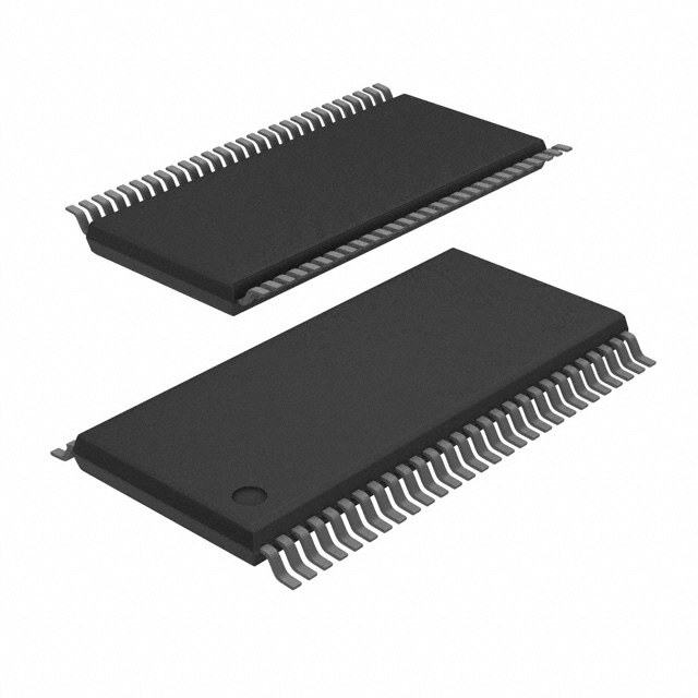
The SN74ALVCH16821DGGR is housed in a 56-pin TSSOP package, ideal for surface mount applications. It boasts an input capacitance of 3.5 pF, which helps in minimizing signal distortion and maintaining high-speed performance. The device is REACH unaffected and RoHS3 compliant, adhering to stringent environmental and safety standards. With a moisture sensitivity level (MSL) of 1 (unlimited), it is well-suited for various manufacturing environments.
SN74ALVCH16821DGGR Features
- High-Speed Performance: With a maximum propagation delay of 4.5ns at 3.3V and 50pF, the SN74ALVCH16821DGGR ensures rapid data processing and minimal latency.
- Low Power Consumption: The device consumes only 40 µA in quiescent mode, making it energy-efficient and suitable for low-power applications.
- Dual Elements: Each element consists of 10 bits, providing a total of 20 bits of storage capacity, which is ideal for applications requiring multiple data storage elements.
- High Output Current: The device supports an output current of 24mA for both high and low states, ensuring strong signal drive capabilities.
- Wide Operating Voltage Range: The 1.65V to 3.6V supply voltage range allows for compatibility with various power supply systems.
- Environmental Compliance: REACH unaffected and RoHS3 compliant, ensuring the device meets global environmental regulations.
- Unlimited Moisture Sensitivity Level: MSL 1 (unlimited) makes the device suitable for a wide range of manufacturing processes without the need for special handling.
SN74ALVCH16821DGGR Applications
The SN74ALVCH16821DGGR is ideal for a variety of high-speed digital applications, including:
- Data Storage and Processing: Its dual 10-bit flip-flops are perfect for storing and processing data in digital systems.
- Clock Management: The high clock frequency and positive edge triggering make it suitable for clock-driven applications.
- Communication Systems: The device's high-speed performance and low power consumption make it ideal for use in communication systems where data integrity and speed are critical.
- Industrial Control Systems: The robust performance and wide operating voltage range make it suitable for industrial applications that require reliable and efficient data handling.
- Consumer Electronics: The device's compliance with environmental standards and its surface mount package make it suitable for consumer electronics where space and environmental impact are considerations.
Conclusion of SN74ALVCH16821DGGR
The SN74ALVCH16821DGGR from Texas Instruments is a high-performance dual 10-bit D-type flip-flop that offers a combination of speed, efficiency, and reliability. Its high clock frequency, low power consumption, and robust environmental compliance make it a versatile choice for a wide range of applications. The device's unique features, such as its low input capacitance and high output current, provide significant advantages over similar models, making it an ideal choice for designers looking to optimize their digital systems. Whether used in data storage, clock management, or communication systems, the SN74ALVCH16821DGGR delivers reliable performance and efficiency.
FAQ
Not available to buy online? Want the lower wholesale price? Please Send RFQ to get best price, we will respond immediately


.png?x-oss-process=image/format,webp/resize,h_32)


