


Texas Instruments
SN74AS574DWR
Flip Flops

Not available to buy online? Want the lower wholesale price? Please Send RFQ to get best price, we will respond immediately


.png?x-oss-process=image/format,webp/resize,p_30)


SN74AS574DWR Description
SN74AS574DWR Description
The SN74AS574DWR is a high-performance, single 8-bit D-type flip-flop from Texas Instruments, designed for a wide range of digital applications. This device operates at a clock frequency of up to 90 MHz, ensuring fast and reliable data processing. It features a positive edge trigger type, which means it captures data on the rising edge of the clock signal, providing precise timing control.
The SN74AS574DWR is built to operate within a supply voltage range of 4.5V to 5.5V, making it suitable for standard 5V digital systems. It offers a maximum propagation delay of just 9ns at 5V and a load capacitance of 50pF, ensuring minimal delay in signal transmission. The device consumes a quiescent current of 116 mA, which is relatively low for its performance capabilities, making it energy-efficient.
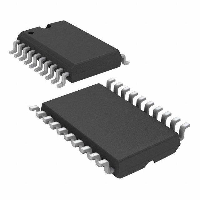
This flip-flop is housed in a surface-mount 20SOIC package, which is ideal for compact and high-density PCB designs. The device is REACH unaffected and RoHS3 compliant, ensuring it meets the latest environmental and safety standards. It has a moisture sensitivity level (MSL) of 1, which means it is not affected by moisture and can be stored without special handling.
SN74AS574DWR Features
- High Clock Frequency: Operates at up to 90 MHz, enabling fast data processing and high-speed applications.
- Positive Edge Triggering: Captures data on the rising edge of the clock signal, ensuring precise timing and synchronization.
- Wide Supply Voltage Range: Functions reliably within a 4.5V to 5.5V supply voltage range, making it compatible with standard 5V digital systems.
- Low Propagation Delay: Achieves a maximum propagation delay of 9ns at 5V and 50pF, minimizing signal delay and improving system performance.
- Low Quiescent Current: Consumes only 116 mA of quiescent current, contributing to energy efficiency.
- High Output Current: Provides 15mA for high output and 48mA for low output, ensuring robust signal drive capabilities.
- Environmental Compliance: REACH unaffected and RoHS3 compliant, meeting stringent environmental and safety standards.
- Moisture Sensitivity Level 1: Can be stored and handled without special moisture protection, simplifying logistics and storage.
- Surface-Mount Packaging: Available in a 20SOIC package, ideal for compact and high-density PCB designs.
SN74AS574DWR Applications
The SN74AS574DWR is well-suited for a variety of applications where high-speed data processing and reliable performance are critical. Some specific use cases include:
- Digital Systems: Ideal for use in digital systems requiring fast and reliable data storage and processing, such as microprocessors, microcontrollers, and digital signal processors.
- Communication Systems: Suitable for applications in communication systems where data integrity and timing are crucial, such as in data transmission and reception circuits.
- Industrial Control: Can be used in industrial control systems for managing and processing digital signals, ensuring precise control and monitoring.
- Consumer Electronics: Applicable in consumer electronics where compact design and high performance are required, such as in smart devices and home automation systems.
- Automotive Electronics: Meets the demands of automotive electronics for reliable and high-speed data processing in applications like engine control units and infotainment systems.
Conclusion of SN74AS574DWR
The SN74AS574DWR from Texas Instruments is a robust and versatile D-type flip-flop that offers high performance and reliability. With its high clock frequency, positive edge triggering, and low propagation delay, it ensures fast and precise data processing. The device's wide supply voltage range, low quiescent current, and high output current make it suitable for a variety of applications, from digital systems to automotive electronics.
Its compliance with environmental and safety standards, along with its moisture sensitivity level of 1, makes it a practical choice for modern electronics design. The surface-mount packaging further enhances its suitability for compact and high-density PCB designs. Overall, the SN74AS574DWR stands out as a reliable and efficient solution for applications requiring high-speed and reliable data processing.
Tech Specifications
SN74AS574DWR Documents
Download datasheets and manufacturer documentation for SN74AS574DWR
SN(5,7)4AS57(4,5),SN(5,7)4ALS574(A,B) SN54/74ALS574B/575A, SN54/74AS574-75 SN(5,7)4AS57(4,5),SN(5,7)4ALS574(A,B) Material Set 21/Jun/2016 Related Parts


Shopping Guide


.png?x-oss-process=image/format,webp/resize,h_32)


©2025 ERSA Electronics Corporation.