
Texas Instruments
SN74AUC1G74DCURE4
Flip Flops


.png?x-oss-process=image/format,webp/resize,p_30)


SN74AUC1G74DCURE4 Description
SN74AUC1G74DCURE4 Description
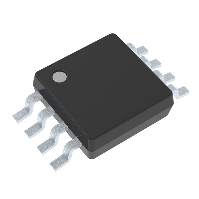
The SN74AUC1G74DCURE4 is a single-bit D-type flip-flop designed for high-performance digital applications. Manufactured by Texas Instruments, this device is part of the 74AUC series and is housed in an 8-VSSOP surface-mount package. It features a clock frequency of up to 275 MHz, making it suitable for high-speed digital circuits. The flip-flop operates with a supply voltage ranging from 0.8V to 2.7V, providing flexibility in power requirements. It supports complementary outputs and is triggered on the positive edge of the clock signal, ensuring reliable and synchronous operation.
SN74AUC1G74DCURE4 Features
- High-Speed Operation: With a clock frequency of up to 275 MHz, the SN74AUC1G74DCURE4 is ideal for high-speed digital systems.
- Low Power Consumption: The device operates within a supply voltage range of 0.8V to 2.7V and has a quiescent current of only 10 µA, making it energy-efficient.
- Complementary Outputs: The flip-flop provides complementary outputs, which can be useful for various digital logic applications.
- Positive Edge Triggering: Ensures synchronous operation and reliable data capture on the rising edge of the clock signal.
- Set and Reset Functionality: The device includes set (preset) and reset functions, allowing for easy initialization and control of the flip-flop state.
- Wide Operating Voltage Range: The 0.8V to 2.7V supply voltage range makes it suitable for a variety of power supply configurations.
- Low Input Capacitance: With an input capacitance of 2.5 pF, the device minimizes loading effects on driving circuits.
- High Output Current Capability: The flip-flop can source and sink up to 9mA, making it capable of driving multiple loads.
- Compliance and Reliability: The SN74AUC1G74DCURE4 is REACH unaffected and RoHS3 compliant, ensuring environmental and regulatory compliance. It also has a moisture sensitivity level (MSL) of 1, making it suitable for extended storage and handling.
SN74AUC1G74DCURE4 Applications
The SN74AUC1G74DCURE4 is well-suited for a variety of applications requiring high-speed, low-power digital storage elements. Some specific use cases include:
- Digital Signal Processing: The high clock frequency and low power consumption make it ideal for digital signal processing applications where speed and efficiency are critical.
- Data Storage and Transfer: The flip-flop can be used in data storage and transfer systems to temporarily hold data bits.
- Control Logic Circuits: The set and reset functions, along with positive edge triggering, make it suitable for control logic circuits in various digital systems.
- Communication Systems: The device can be used in communication systems for data synchronization and buffering.
- Consumer Electronics: The low power consumption and wide operating voltage range make it suitable for consumer electronics where power efficiency and flexibility are important.
Conclusion of SN74AUC1G74DCURE4
The SN74AUC1G74DCURE4 from Texas Instruments is a versatile and high-performance D-type flip-flop designed for modern digital applications. Its high clock frequency, low power consumption, and complementary outputs make it a reliable choice for various digital circuits. The inclusion of set and reset functions, along with its wide operating voltage range and low input capacitance, further enhance its utility. The device's compliance with environmental and regulatory standards ensures its suitability for a broad range of applications. Whether used in digital signal processing, data storage, or control logic circuits, the SN74AUC1G74DCURE4 offers a robust and efficient solution for digital storage and control needs.
Tech Specifications
SN74AUC1G74DCURE4 Documents
Download datasheets and manufacturer documentation for SN74AUC1G74DCURE4
 SN74AUC1G74YZPR Datasheet
  SN74AUC1G74YZPR Datasheet
 Shopping Guide


.png?x-oss-process=image/format,webp/resize,h_32)


