
Texas Instruments
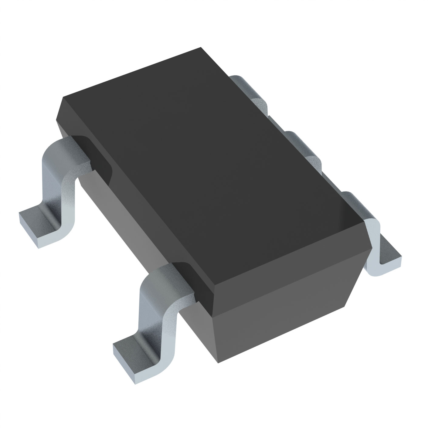
SN74AUP1G08DBVR
Gates and Inverters


- 5+
- $0.17357
- $0.87
- 50+
- $0.14156
- $7.08
- 150+
- $0.12784
- $19.18
- 500+
- $0.11071
- $55.36
- 3000+
- $0.09606
- $288.18
- 6000+
- $0.09150
- $549

.png?x-oss-process=image/format,webp/resize,p_30)


SN74AUP1G08DBVR Description
The Texas Instruments SN74AUP1G08DBVR is a high-speed Si-gate transistor-transistor logic (TTL) device that features an open-drain output configuration. This device is designed to provide high-speed switching and low power consumption, making it suitable for a wide range of applications.
Description:
The SN74AUP1G08DBVR is a quad 2-input AND gate with open-drain outputs. It is available in a compact SOT23-5 package, making it ideal for use in space-constrained applications. The device operates over a wide supply voltage range of 2.0V to 6.0V and has a maximum output current of -25 mA.
Features:
- Open-drain outputs: The open-drain outputs allow for easy interfacing with other open-drain devices or systems that require an open-collector configuration.
- High-speed switching: The device is designed for high-speed operation, with a propagation delay of 3.5 ns (typical) and a rise and fall time of 2.0 ns (typical).
- Low power consumption: The SN74AUP1G08DBVR has a low power consumption of 2.2 mW per gate at a supply voltage of 5V, making it suitable for battery-powered applications.
- Wide supply voltage range: The device operates over a supply voltage range of 2.0V to 6.0V, making it compatible with various power supply systems.
- SOT23-5 package: The compact SOT23-5 package allows for easy integration into small form-factor applications.
Applications:
- Digital circuits: The SN74AUP1G08DBVR can be used in various digital circuits, such as logic gates, decoders, and encoders, where high-speed switching and low power consumption are required.
- Battery-powered devices: Due to its low power consumption, the device is suitable for use in battery-powered applications, such as portable electronics and wireless communication devices.
- Industrial control systems: The device can be used in industrial control systems where high-speed switching and reliable operation are essential.
- Automotive applications: The SN74AUP1G08DBVR can be used in automotive applications, such as infotainment systems and control modules, where space constraints and low power consumption are critical.
- Medical equipment: The device can be used in medical equipment, such as monitoring devices and diagnostic equipment, where high-speed processing and low power consumption are important.
In summary, the Texas Instruments SN74AUP1G08DBVR is a high-speed, low-power quad 2-input AND gate with open-drain outputs. Its compact package, wide supply voltage range, and low power consumption make it suitable for a wide range of applications, including digital circuits, battery-powered devices, industrial control systems, automotive applications, and medical equipment.
Tech Specifications
SN74AUP1G08DBVR Documents
Download datasheets and manufacturer documentation for SN74AUP1G08DBVR
 Multi Dev 29/Sep/2022
  SN74AUP1G08 Logic Guide
  SN74AUP1G08 Logic Guide
  Die Conversion Revision A 19/Feb/2015 Die Conversion 09/Oct/2014
 Shopping Guide


.png?x-oss-process=image/format,webp/resize,h_32)


