
Texas Instruments
SN74AUP1G08DCKT
Gates and Inverters


.png?x-oss-process=image/format,webp/resize,p_30)


SN74AUP1G08DCKT Description
SN74AUP1G08DCKT Description
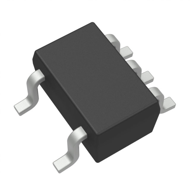
The SN74AUP1G08DCKT from Texas Instruments is a single 2-input AND gate in the 74AUP series, designed for ultra-low-power operation in 0.8V to 3.6V supply voltage environments. Packaged in a compact SC70-5 surface-mount form factor, this logic gate is optimized for portable and battery-powered applications where minimal power consumption and space efficiency are critical. With a maximum propagation delay of 6.2ns at 3.3V and 30pF load, it balances speed and power efficiency, making it ideal for modern digital systems.
SN74AUP1G08DCKT Features
- Ultra-Low Power: Quiescent current as low as 500nA ensures minimal power drain in standby modes.
- Wide Voltage Range: Operates from 0.8V to 3.6V, supporting mixed-voltage designs.
- High Noise Immunity: Input logic levels (0.7V–0.9V for LOW, 1.6V–2V for HIGH) enhance robustness in noisy environments.
- Balanced Output Drive: 4mA output current (sink/source) ensures reliable signal integrity.
- Space-Saving: SC70-5 package (1.25mm × 2mm) is ideal for compact PCB layouts.
- RoHS3 & REACH Compliant: Meets stringent environmental and safety standards.
SN74AUP1G08DCKT Applications
- Battery-Powered Devices: Wearables, IoT sensors, and handheld electronics benefit from its low-voltage operation and minimal power consumption.
- Signal Conditioning: Used in level shifting and logic interfacing between mixed-voltage domains (e.g., 1.8V to 3.3V).
- Portable Consumer Electronics: Smartphones, tablets, and wireless peripherals leverage its small footprint and efficiency.
- Industrial Control Systems: Reliable performance in low-voltage PLCs and sensor interfaces.
Conclusion of SN74AUP1G08DCKT
The SN74AUP1G08DCKT stands out for its ultra-low power, wide voltage range, and robust performance in space-constrained designs. Its combination of speed, efficiency, and environmental compliance makes it a superior choice for modern digital and mixed-signal systems. Engineers designing for portable, battery-operated, or noise-sensitive applications will find this AND gate an optimal solution.
Tech Specifications
SN74AUP1G08DCKT Documents
Download datasheets and manufacturer documentation for SN74AUP1G08DCKT
 SN74AUP1G08 Logic Guide
  SN74AUP1G08 Logic Guide
  Die Conversion Revision A 19/Feb/2015 Die Conversion 09/Oct/2014
 Shopping Guide


.png?x-oss-process=image/format,webp/resize,h_32)


