
 German
 Japanese
 Portuguese
 Korea
Korea
 Mexico
 Dutch
Dutch


Texas Instruments
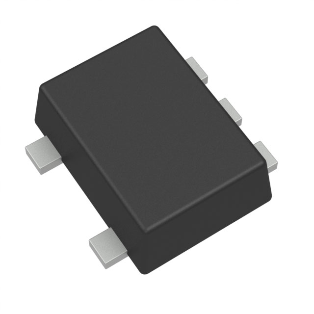
SN74AUP1G08DRLR

Why Choose Us?
Professional Platform
B2B & B2C purchasingDelivery at full speed
1-2 days deliveryWide variety
Original manufacturers365 days guarantee
Responsible quality
.png)


Tech Specifications
SN74AUP1G08DRLR Description
The SN74AUP1G08DRLR is a high-speed Si-gate CMOS device manufactured by Texas Instruments. It is a quad 2-input AND gate, which means it has four independent AND gate functions in a single package. Here is a brief description of the model, its features, and applications:
Description:
The SN74AUP1G08DRLR is a member of the 74AUP1G series of high-speed Si-gate CMOS devices. It is a quad 2-input AND gate, which performs logical AND operations on two binary inputs and produces a single binary output. The device is designed for use in a wide range of digital applications where high-speed operation is required.
Features:
- High-Speed Operation: The device is designed for high-speed operation, making it suitable for applications that require quick response times.
- Low Power Consumption: The SN74AUP1G08DRLR operates at low power levels, which is beneficial for battery-powered or power-sensitive applications.
- Si-gate CMOS Technology: The use of Si-gate CMOS technology provides high noise immunity and ensures reliable operation in various environments.
- Quad 2-input AND Gates: The device contains four independent AND gates, allowing for multiple logical operations within a single package.
- Wide Supply Voltage Range: The SN74AUP1G08DRLR can operate over a wide range of supply voltages, making it versatile for different power supply conditions.
- Logic Level Compatibility: The device is compatible with both TTL and CMOS logic families, allowing for easy integration with various digital systems.
Applications:
- Digital Logic Circuits: The SN74AUP1G08DRLR can be used to construct various digital logic circuits, such as combinational and sequential circuits, for performing complex logical operations.
- Automotive Electronics: Due to its high-speed operation and low power consumption, the device is suitable for use in automotive electronics, such as control systems and communication interfaces.
- Telecommunications: The device can be used in high-speed telecommunications equipment, where quick processing of digital signals is essential.
- Industrial Control Systems: The SN74AUP1G08DRLR can be utilized in industrial control systems for signal processing and decision-making tasks.
- Computing and Data Processing: The device can be employed in computing and data processing applications, such as arithmetic logic units (ALUs) and memory control circuits.
- Consumer Electronics: The SN74AUP1G08DRLR can be used in consumer electronics, such as gaming consoles, smartphones, and home automation systems, for various digital logic functions.
In summary, the SN74AUP1G08DRLR is a versatile, high-speed quad 2-input AND gate that offers low power consumption and compatibility with both TTL and CMOS logic families. Its features make it suitable for a wide range of digital applications, from digital logic circuits to high-speed telecommunications equipment.
FAQ
| Quantity | Unit Price | Ext. Price |
|---|---|---|
| 1+ | $0.34320 | $0.34 |
| 10+ | $0.23936 | $2.39 |
| 25+ | $0.21296 | $5.32 |
| 100+ | $0.18410 | $18.41 |
| 250+ | $0.17033 | $42.58 |
Not available to buy online? Want the lower wholesale price? Please Send RFQ to get best price, we will respond immediately


.png?x-oss-process=image/format,webp/resize,h_32)


