
 German
 Japanese
 Portuguese
 Korea
Korea
 Mexico
 Dutch
Dutch


Texas Instruments
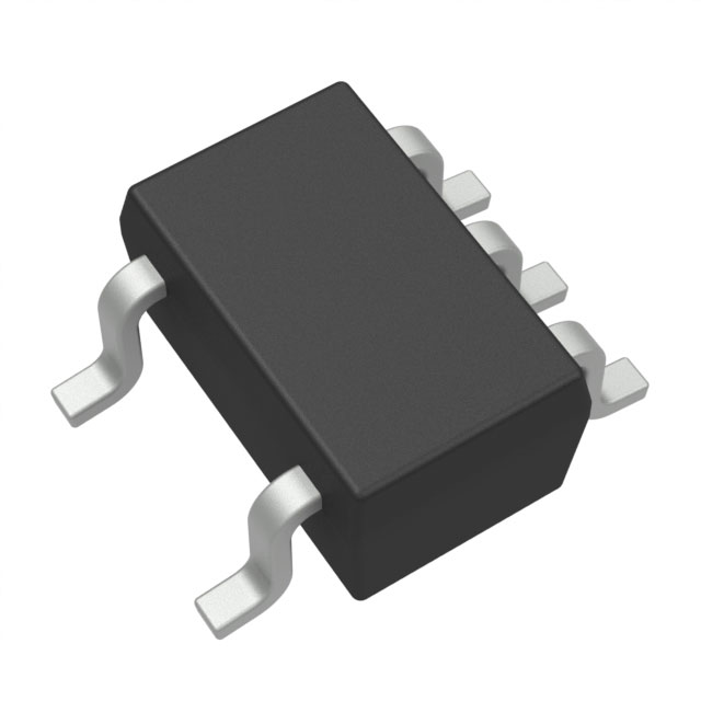
SN74AUP1G34DCKR

Why Choose Us?
Professional Platform
B2B & B2C purchasingDelivery at full speed
1-2 days deliveryWide variety
Original manufacturers365 days guarantee
Responsible quality
.png)


Tech Specifications
SN74AUP1G34DCKR Description
The Texas Instruments SN74AUP1G34DCKR is a single-pole, double-throw (SPDT) analog switch. It is a part of the 74AUP1Gxx series of analog switches, which are designed to provide high performance and low power consumption in a small package.
Description:
The SN74AUP1G34DCKR is a digital-input, single-pole double-throw analog switch with true analog signal routing. It is available in a small DFN (Dual Flat No-Leads) package, making it ideal for use in portable and battery-powered applications. The switch has a low on-impedance of 50 ohms, which helps to minimize signal loss and distortion.
Features:
- Ultra-low power consumption: The SN74AUP1G34DCKR consumes only 2.5uA of supply current, making it ideal for use in battery-powered applications.
- Wide supply voltage range: The switch can operate from a supply voltage range of 1.65V to 5.5V, making it suitable for use in a variety of applications.
- Low on-impedance: The switch has a low on-impedance of 50 ohms, which helps to minimize signal loss and distortion.
- True analog signal routing: The switch provides true analog signal routing, which means that it can handle both AC and DC signals without any distortion.
- Small package: The switch is available in a small DFN package, making it ideal for use in portable and battery-powered applications.
Applications:
The SN74AUP1G34DCKR is suitable for a wide range of applications, including:
- Audio switching in portable devices
- Battery-powered measurement equipment
- Audio mixers and amplifiers
- Medical equipment
- Industrial control systems
- Wireless communication systems
In summary, the Texas Instruments SN74AUP1G34DCKR is a high-performance, low-power analog switch that is ideal for use in a variety of applications, including audio switching, battery-powered measurement equipment, and wireless communication systems. Its small package size and low on-impedance make it a popular choice for portable and battery-powered applications.
FAQ
| Quantity | Unit Price | Ext. Price |
|---|---|---|
| 5+ | $0.13032 | $0.65 |
| 50+ | $0.12751 | $6.38 |
| 150+ | $0.12563 | $18.84 |
| 500+ | $0.12376 | $61.88 |
Not available to buy online? Want the lower wholesale price? Please Send RFQ to get best price, we will respond immediately


.png?x-oss-process=image/format,webp/resize,h_32)


