
 German
 Japanese
 Portuguese
 Korea
Korea
 Mexico
 Dutch
Dutch


Texas Instruments
SN74AUP1G80YZPR

Why Choose Us?
Professional Platform
B2B & B2C purchasingDelivery at full speed
1-2 days deliveryWide variety
Original manufacturers365 days guarantee
Responsible quality
.png)


Tech Specifications
SN74AUP1G80YZPR Description
SN74AUP1G80YZPR Description
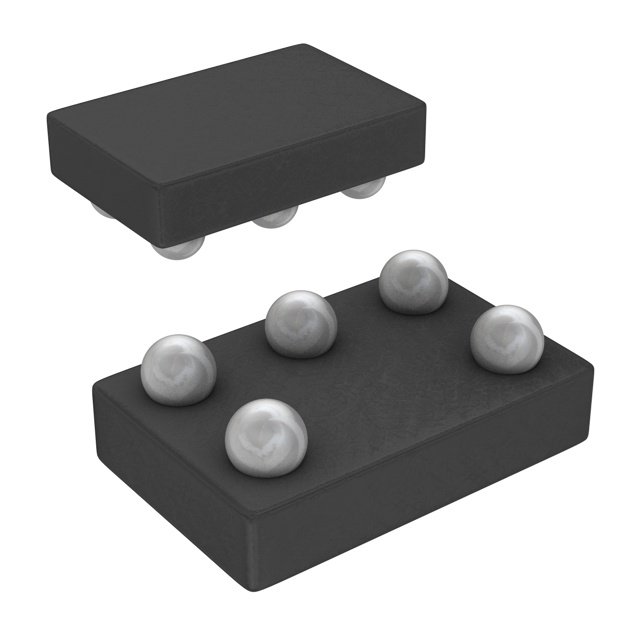
The SN74AUP1G80YZPR is a single-bit D-type flip-flop integrated circuit (IC) designed by Texas Instruments. This logic IC chip belongs to the 74AUP and series is packaged in a 5-DSBGA format, making it suitable for surface-mount applications. Despite being marked as obsolete, the SN74AUP1G80YZPR remains a reliable choice for various digital logic applications due to its robust performance and versatile operating conditions.
SN74AUP1G80YZPR Features
- Clock Frequency: The SN74AUP1G80YZPR operates at a clock frequency of up to 260 MHz, ensuring high-speed data processing and synchronization.
- Output Type: It features an inverted output, which is useful for applications requiring signal inversion.
- Trigger Type: The flip-flop is triggered on the positive edge of the clock signal, providing precise timing control.
- Voltage - Supply: The IC operates within a wide voltage range of 0.8V to 3.6V, making it compatible with various power supply configurations.
- Max Propagation Delay: At 3.3V and a maximum load capacitance of 30pF, the maximum propagation delay is 6.4ns, ensuring fast signal transmission.
- Current - Quiescent (Iq): The quiescent current is as low as 500 nA, contributing to energy efficiency.
- Input Capacitance: The low input capacitance of 1.5 pF minimizes loading effects on driving circuits.
- Current - Output High, Low: The output current capability is balanced at 4mA for both high and low states, ensuring stable signal levels.
- Moisture Sensitivity Level (MSL): With an MSL of 1 (unlimited), the IC is suitable for a wide range of environmental conditions.
- Compliance: The SN74AUP1G80YZPR is REACH unaffected and ROHS3 compliant, adhering to stringent environmental and safety standards.
SN74AUP1G80YZPR Applications
The SN74AUP1G80YZPR is ideal for applications requiring high-speed, single-bit data storage and synchronization. Its features make it suitable for:
- Digital Signal Processing: The high clock frequency and low propagation delay ensure efficient processing of digital signals.
- Data Storage and Retrieval: The D-type flip-flop is well-suited for temporary data storage and retrieval operations.
- Clock Synchronization: The positive edge triggering mechanism allows precise synchronization with clock signals.
- Low-Power Applications: The low quiescent current and wide voltage range make it suitable for battery-operated or energy-efficient systems.
Conclusion of SN74AUP1G80YZPR
The SN74AUP1G80YZPR, despite being obsolete, remains a valuable component in the electronics industry due to its high performance and versatility. Its wide operating voltage range, low quiescent current, and fast propagation delay make it an excellent choice for a variety of digital logic applications. The IC's compliance with environmental and safety standards further enhances its appeal. For applications requiring reliable single-bit data storage and synchronization, the SN74AUP1G80YZPR is a robust and efficient solution.
FAQ
Not available to buy online? Want the lower wholesale price? Please Send RFQ to get best price, we will respond immediately


.png?x-oss-process=image/format,webp/resize,h_32)


