
 German
 Japanese
 Portuguese
 Korea
Korea
 Mexico
 Dutch
Dutch


Texas Instruments
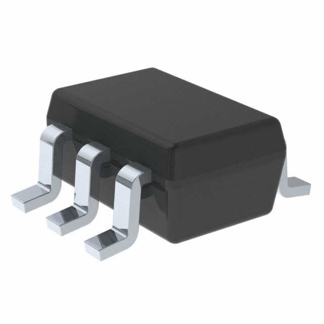
SN74AUP2G06DCKR

Why Choose Us?
Professional Platform
B2B & B2C purchasingDelivery at full speed
1-2 days deliveryWide variety
Original manufacturers365 days guarantee
Responsible quality
.png)


Tech Specifications
SN74AUP2G06DCKR Description
SN74AUP2G06DCKR Description
The SN74AUP2G06DCKR from Texas Instruments is a dual-channel inverter IC with open-drain outputs, designed for low-voltage, low-power applications. Part of the 74AUP series, it operates across a wide supply voltage range of 0.8V to 3.6V, making it suitable for battery-powered and portable electronics. With a maximum propagation delay of 10.5ns at 3.3V and 30pF load, it ensures reliable signal inversion in high-speed digital circuits. The device features two independent inverters, each with a single input, and offers open-drain outputs for flexible interfacing with other logic levels or driving loads directly.
SN74AUP2G06DCKR Features
- Low Power Consumption: Quiescent current as low as 500nA maximizes energy efficiency in power-sensitive designs.
- Wide Voltage Range: Supports 0.8V–3.6V operation, ideal for mixed-voltage systems.
- Open-Drain Outputs: Enable wired-AND configurations and easy interfacing with higher-voltage devices.
- High Noise Immunity: Input logic levels (0.7V–0.9V for LOW, 1.6V–2V for HIGH) ensure robust performance in noisy environments.
- Compact Packaging: Housed in an SC70-6 package, it saves board space in dense PCB layouts.
- RoHS3 & REACH Compliant: Meets environmental and regulatory standards for global deployment.
SN74AUP2G06DCKR Applications
- Portable Electronics: Ideal for smartphones, wearables, and IoT devices due to ultra-low power consumption.
- Level Shifting: Open-drain outputs facilitate voltage translation between 1.8V, 2.5V, and 3.3V logic domains.
- Signal Conditioning: Used in sensor interfaces and communication modules for signal inversion and buffering.
- Industrial Control Systems: Reliable performance in harsh environments with high noise immunity.
- Automotive Electronics: Suitable for infotainment and control units, leveraging its wide operating voltage range.
Conclusion of SN74AUP2G06DCKR
The SN74AUP2G06DCKR stands out for its low-voltage operation, minimal power draw, and flexible open-drain outputs, making it a versatile choice for modern digital designs. Its small footprint and robust performance cater to applications ranging from consumer electronics to industrial automation. Engineers benefit from its high noise tolerance and compliance with environmental standards, ensuring reliability in diverse use cases. For designers seeking a space-efficient, energy-conscious inverter solution, this IC delivers exceptional value.
FAQ
Not available to buy online? Want the lower wholesale price? Please Send RFQ to get best price, we will respond immediately


.png?x-oss-process=image/format,webp/resize,h_32)


