Texas Instruments_SN74AUP2G17DCKR

Texas Instruments
SN74AUP2G17DCKR  
Buffers, Drivers, Receivers, Transceivers

Texas Instruments
SN74AUP2G17DCKR
704-SN74AUP2G17DCKR
Ersa
Texas Instruments-SN74AUP2G17DCKR-datasheets-3058838.pdf
IC BUF NON-INVERT 3.6V SC70-6
In Stock : 38533

Not available to buy online? Want the lower wholesale price? Please Send RFQ to get best price, we will respond immediately

QUICK RFQ
ADD TO RFQ LIST
ersa FreeSample ersa flow
  • Quantity
  • Unit Price
  • Ext. Price
    • 1+
    • $0.30470
    • $0.3
    • 10+
    • $0.23018
    • $2.3
    • 30+
    • $0.19872
    • $5.96
    • 100+
    • $0.15898
    • $15.9
    • 500+
    • $0.14076
    • $70.38
    • 1000+
    • $0.12917
    • $129.17
    ADD TO CART
    QUICK ORDER
    $0.30470    $0.30
    ISO9001
    Quality Policy
    ISO45001
    ISO14001

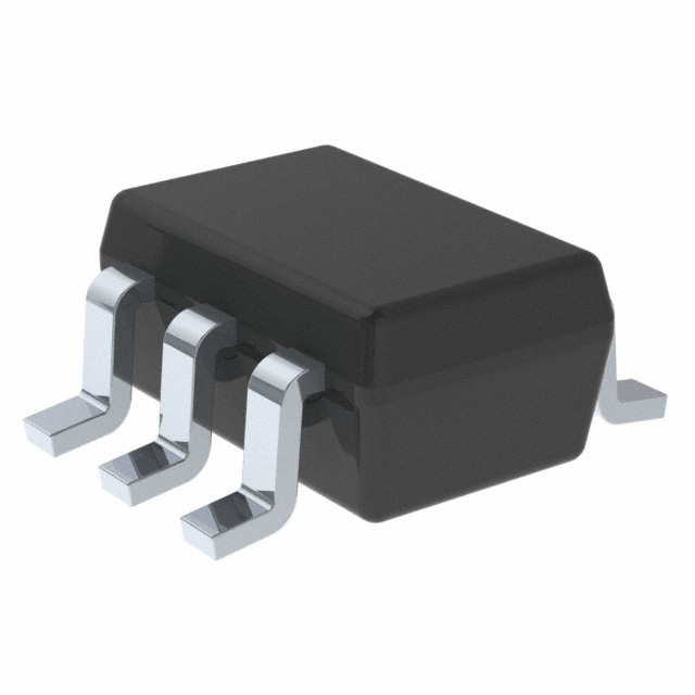
    SN74AUP2G17DCKR Description

    The SN74AUP2G17DCKR is a high-speed dual 2-input multiplexer (MUX) manufactured by Texas Instruments. It is part of the 74AUP2G17 series, which offers high-speed performance and low power consumption. Here's a brief description, features, and applications of the SN74AUP2G17DCKR:

    Description:

    The SN74AUP2G17DCKR is a dual 2-input multiplexer integrated circuit (IC) designed for high-speed applications. It allows two input signals to be selected and routed to a single output based on the state of a select input. The device is available in a small DFN (Dual Flat No-leads) package, making it suitable for compact and space-constrained applications.

    Features:

    1. High-speed performance: The SN74AUP2G17DCKR operates at high speeds, with a propagation delay of typically 2.7 ns (typical) and a minimum input pulse width of 2.7 ns (typical).
    2. Low power consumption: The device has a low power consumption of 3.4 mW per multiplexer (typical) at a supply voltage of 3.3V.
    3. Wide supply voltage range: It operates over a supply voltage range of 1.65V to 5.5V, making it suitable for various applications with different power requirements.
    4. Small package: The DFN package is compact and suitable for space-constrained applications.
    5. High input impedance: The device has high input impedance, which reduces the loading on the driving circuit.
    6. TTL and CMOS compatible: The SN74AUP2G17DCKR is compatible with both TTL and CMOS logic families.

    Applications:

    1. Digital signal processing: The high-speed performance of the SN74AUP2G17DCKR makes it suitable for use in digital signal processing applications, such as audio or video processing systems.
    2. Telecommunications: The device can be used in high-speed telecommunications equipment, such as routers, switches, and modems.
    3. Data acquisition systems: The SN74AUP2G17DCKR can be used in data acquisition systems where high-speed signal routing and selection are required.
    4. Industrial control systems: The device can be used in industrial control systems for routing and selecting signals in complex control circuits.
    5. Test and measurement equipment: The high-speed performance and low power consumption make the SN74AUP2G17DCKR suitable for use in test and measurement equipment, such as oscilloscopes and logic analyzers.

    In summary, the SN74AUP2G17DCKR is a high-speed, low-power dual 2-input multiplexer from Texas Instruments, suitable for various applications requiring high-speed signal routing and selection, such as digital signal processing, telecommunications, data acquisition systems, industrial control systems, and test and measurement equipment.

    Tech Specifications

    Number of Channels per Chip
    Number of Output Enables per Chip
    Unit Weight
    Maximum Quiescent Current (uA)
    PPAP
    Automotive
    RoHS
    Maximum High Level Output Current (mA)
    Absolute Propagation Delay Time (ns)
    REACH Status
    Output type
    Maximum Operating Supply Voltage (V)
    Operating temperature range (°C)
    Supplier Temperature Grade
    Standard Package Name
    High Level Output Current
    Mounting
    Input Signal Type
    Typical Operating Supply Voltage (V)
    Package
    IOH (max) (mA)
    Current - Output High, Low
    Output Type
    Supply Current - Max
    Process Technology
    Package Height
    Maximum Operating Temperature
    Width
    RoHS Status
    Number of channels
    Number of Inputs per Chip
    Number of Input Lines
    Maximum Low Level Output Current (mA)
    Minimum Operating Temperature
    Number of Input Enables per Chip
    Length
    Operating Supply Voltage
    Part Status
    Lead finish / Ball material
    Package Width
    Supply voltage (min) (V)
    Product Status
    Supplier Package
    Package / Case
    Number of Channels
    Technology
    Voltage - Supply
    Logic Function
    Number of Elements
    EU RoHS
    Carrier
    Moisture Sensitivity Level (MSL)
    Operating Temperature
    Tolerant I/Os (V)
    Logic Type
    ECCN
    MSL rating / Peak reflow
    Mounting Type
    Pin Count
    Lead Shape
    SVHC
    Quiescent Current
    Low Level Output Current
    HTSUS
    Pins
    USHTS
    Propagation Delay Time
    PCB changed
    HTS
    Number of Elements per Chip
    Rating
    ECCN (US)
    Supply current (max) (µA)
    Supplier Device Package
    Supply Voltage - Min
    Minimum Operating Temperature (°C)
    Maximum Operating Temperature (°C)
    Function
    Operating Supply Current
    Propagation Delay Test Condition (pF)
    Mfr
    Polarity
    Supply voltage (max) (V)
    Height
    Features
    Supply Voltage - Max
    Mounting Style
    Input Type
    Technology family
    Number of Bits per Element
    Number of Outputs per Chip
    Package Length
    REACH
    Series
    Input type
    Number of Output Lines
    IOL (max) (mA)
    Bus Hold
    Logic Family
    Base Product Number
    Minimum Operating Supply Voltage (V)

    SN74AUP2G17DCKR Documents

    Download datasheets and manufacturer documentation for SN74AUP2G17DCKR

    Ersa Assembly Site 24/Apr/2023      
    Ersa SN74AUP2G17      
    Ersa SN74AUP2G17      
    Ersa Copper Bond Wire 07/May/2014       Copper Wire Revision A 03/Nov/2014      

    Shopping Guide

    Payment Methods
    Payment Methods include Prepayment TT (bank transfer), Western Union, and PayPal. Customers are responsible for shipping costs, bank charges, customs duties and taxes.
    Shipping Rate
    Shipments are made once a day around 5pm, excluding Sundays. Once shipped, the estimated delivery time is usually 5-7 business days, depending on the courier you choose.
    Delivery Methods
    Provide DHL, FedEx, UPS, EMS, SF Express and Registered Airmail International Delivery Service