
 German
 Japanese
 Portuguese
 Korea
Korea
 Mexico
 Dutch
Dutch


Texas Instruments
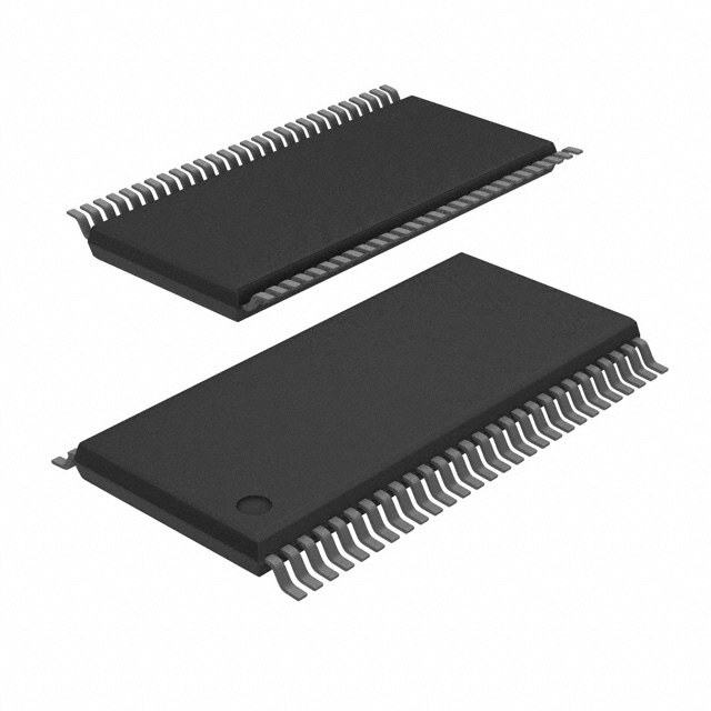
SN74CBT16211ADGGR

Why Choose Us?
Professional Platform
B2B & B2C purchasingDelivery at full speed
1-2 days deliveryWide variety
Original manufacturers365 days guarantee
Responsible quality
.png)


Tech Specifications
SN74CBT16211ADGGR Description
The Texas Instruments SN74CBT16211ADGGR is a high-speed CMOS 4-to-1 multiplexer/Demultiplexer. The device is designed to be used in a variety of applications, including digital signal processing, data routing, and communication systems.
Description:
The SN74CBT16211ADGGR is a member of the 74CBT16200 series of logic devices. It is a 4-to-1 multiplexer/Demultiplexer, which means it can be used to select one of four input signals and route it to a single output, or to distribute a single input signal to one of four outputs. The device is available in a 16-pin QFN package.
Features:
- 4-to-1 multiplexer/Demultiplexer functionality
- High-speed CMOS design
- 16-pin QFN package
- Low power consumption
- Wide operating voltage range (2.0V to 3.6V)
- High input impedance
- Low output impedance
- Fast switching times (tYP\ _switch = 4.5ns)
Applications:
The SN74CBT16211ADGGR is suitable for a wide range of applications, including:
- Digital signal processing: The device can be used to select one of four input signals and route it to a single output, which can be useful in digital signal processing applications.
- Data routing: The device can be used to distribute a single input signal to one of four outputs, which can be useful in data routing applications.
- Communication systems: The device can be used to select one of four communication channels and route it to a single output, which can be useful in communication systems.
- Logic control: The device can be used in logic control applications, where it can be used to select one of four input signals based on the state of the control inputs.
- Test and measurement: The device can be used in test and measurement applications, where it can be used to select one of four input signals for testing or measurement.
Overall, the SN74CBT16211ADGGR is a versatile and high-performance multiplexer/Demultiplexer that can be used in a variety of digital applications. Its high-speed CMOS design, low power consumption, and fast switching times make it an ideal choice for demanding applications.
FAQ
| Quantity | Unit Price | Ext. Price |
|---|---|---|
| 1+ | $8.94172 | $8.94 |
| 10+ | $8.71715 | $87.17 |
| 30+ | $8.56800 | $257.04 |
Not available to buy online? Want the lower wholesale price? Please Send RFQ to get best price, we will respond immediately


.png?x-oss-process=image/format,webp/resize,h_32)


