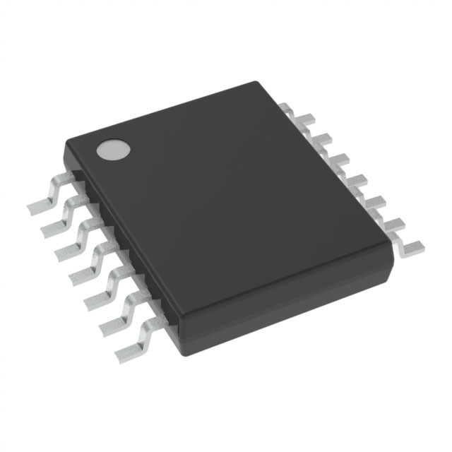
Texas Instruments_SN74HC08QPWRG4Q1

Texas Instruments
SN74HC08QPWRG4Q1  
Gates and Inverters

Texas Instruments
SN74HC08QPWRG4Q1
705-SN74HC08QPWRG4Q1
Ersa
Texas Instruments-SN74HC08QPWRG4Q1-datasheets-1344127.pdf
IC GATE AND 4CH 2-INP 14TSSOP
In Stock : 2791

Not available to buy online? Want the lower wholesale price? Please Send RFQ to get best price, we will respond immediately

QUICK RFQ
ADD TO RFQ LIST
ersa FreeSample ersa flow
ISO9001
Quality Policy
ISO45001
ISO14001

SN74HC08QPWRG4Q1 Description

The SN74HC08QPWRG4Q1 is a quad 2-input AND gate integrated circuit (IC) manufactured by Texas Instruments. It belongs to the family of high-speed Si-gate CMOS logic devices. Here's a brief description, features, and applications of the SN74HC08QPWRG4Q1:

Description:

The SN74HC08QPWRG4Q1 is a quad 2-input AND gate, which means it consists of four independent AND gate circuits in a single 14-pin Quad Flat No-Lead (QFN) package. Each AND gate has two input terminals and one output terminal. The output is HIGH only when both inputs are HIGH.

Features:

  1. 14-pin QFN package
  2. CMOS technology for low power consumption
  3. High-speed Si-gate CMOS logic
  4. Wide operating voltage range: 2.0V to 6.0V
  5. High noise immunity
  6. Suitable for general-purpose digital applications
  7. RoHS compliant

Applications:

  1. Digital logic circuits: The SN74HC08QPWRG4Q1 can be used to implement various digital logic functions, such as combinational and sequential circuits, due to its AND gate functionality.
  2. Signal processing: It can be used in signal processing applications where AND operations are required, such as in digital filters or multiplexers.
  3. Microcontroller input/output expansion: The AND gates can be used to expand the input/output capabilities of microcontrollers or other digital systems.
  4. Data validation: The SN74HC08QPWRG4Q1 can be used to validate data inputs in digital systems, ensuring that certain conditions are met before proceeding with further processing.
  5. Logic conversion: It can be used to convert between different logic families, such as TTL and CMOS, due to its compatibility with a wide range of operating voltages.

The SN74HC08QPWRG4Q1 is a versatile and widely used digital logic IC that can be easily integrated into various digital applications, thanks to its compact package, low power consumption, and high-speed performance.

Tech Specifications

Unit Weight
Maximum Propagation Delay Time @ Maximum CL (ns)
Maximum Quiescent Current (uA)
Product
PPAP
Automotive
RoHS
Maximum High Level Output Current (mA)
Absolute Propagation Delay Time (ns)
REACH Status
Number of Inputs
Output type
Number of Element Outputs
Maximum Operating Supply Voltage (V)
Number of Bits
Max Propagation Delay @ V, Max CL
Operating temperature range (°C)
Supplier Temperature Grade
Standard Package Name
High Level Output Current
Mounting
Qualification
Input Logic Level - High
Typical Operating Supply Voltage (V)
Package
IOH (max) (mA)
Current - Output High, Low
Output Type
Process Technology
Package Height
Maximum Operating Temperature
Width
RoHS Status
Current - Quiescent (Max)
Number of channels
Data rate (max) (Mbps)
Number of Input Lines
Number of Element Inputs
Input Logic Level - Low
Maximum Low Level Output Current (mA)
Minimum Operating Temperature
Number of Output Enables per Element
Length
Operating Supply Voltage
Part Status
Lead finish / Ball material
Number of Circuits
Package Width
Supply voltage (min) (V)
Product Status
Supplier Package
Package / Case
Voltage - Supply
Logic Function
Inputs per channel
EU RoHS
Carrier
Moisture Sensitivity Level (MSL)
Operating Temperature
Logic Type
Output Current
ECCN
Grade
MSL rating / Peak reflow
Mounting Type
Pin Count
Lead Shape
Number of Gates
Low Level Output Current
HTSUS
Pins
USHTS
Output Voltage
Propagation Delay Time
PCB changed
HTS
Number of Elements per Chip
Rating
ECCN (US)
Supplier Device Package
Supply Voltage - Min
Minimum Operating Temperature (°C)
Maximum Operating Temperature (°C)
Function
Operating Supply Current
Propagation Delay Test Condition (pF)
Mfr
Supply voltage (max) (V)
Features
Height
Number of Selection Inputs per Element
Supply Voltage - Max
Mounting Style
Input Type
Technology family
Package Length
REACH
Series
Input type
Number of Output Lines
IOL (max) (mA)
Logic Family
Base Product Number
Minimum Operating Supply Voltage (V)

SN74HC08QPWRG4Q1 Documents

Download datasheets and manufacturer documentation for SN74HC08QPWRG4Q1

Ersa Mult Dev 26/Mar/2020      
Ersa SN74HC08-Q1      
Ersa SN74HC08-Q1      
Ersa New Assembly Materials 02/Nov/2016       Design 22/Feb/2022      

Shopping Guide

Payment Methods
Payment Methods include Prepayment TT (bank transfer), Western Union, and PayPal. Customers are responsible for shipping costs, bank charges, customs duties and taxes.
Shipping Rate
Shipments are made once a day around 5pm, excluding Sundays. Once shipped, the estimated delivery time is usually 5-7 business days, depending on the courier you choose.
Delivery Methods
Provide DHL, FedEx, UPS, EMS, SF Express and Registered Airmail International Delivery Service