
 German
 Japanese
 Portuguese
 Korea
Korea
 Mexico
 Dutch
Dutch


Texas Instruments
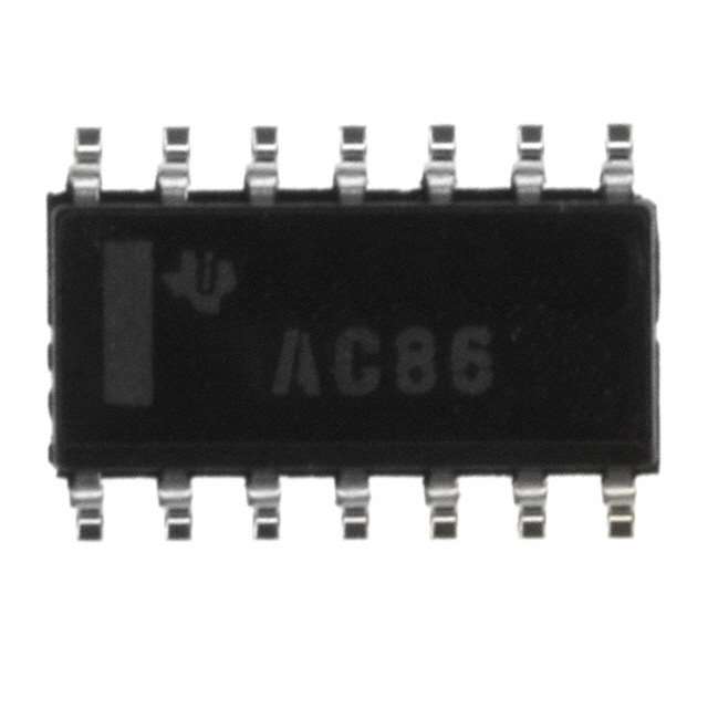
SN74HC14ADBR

Why Choose Us?
Professional Platform
B2B & B2C purchasingDelivery at full speed
1-2 days deliveryWide variety
Original manufacturers365 days guarantee
Responsible quality
.png)


Tech Specifications
SN74HC14ADBR Description
SN74HC14ADBR Description
The SN74HC14ADBR is a high-performance, hex Schmitt-trigger inverter from Texas Instruments, designed for a wide range of digital logic applications. This device is part of the 74HC series, known for its robustness and reliability in various electronic circuits. The SN74HC14ADBR features six independent inverter circuits, each equipped with Schmitt-trigger inputs to provide noise immunity and reliable switching characteristics.
Key technical specifications include a maximum propagation delay of 19ns at 6V and a maximum load capacitance of 50pF. The device operates within a supply voltage range of 2V to 6V, making it suitable for a variety of power supply conditions. The input logic levels are defined as low (0.1V to0.26V) and high (1.9V to 5.9V), ensuring compatibility with standard digital logic systems. The maximum quiescent current is a low 2 µA, and the output current capability is 5.2mA for both high and low states.
The SN74HC14ADBR is available in a surface-mount package, making it ideal for compact and high-density PCB designs. It is RoHS3 compliant and REACH unaffected, ensuring environmental sustainability and regulatory compliance. The device also has a moisture sensitivity level (MSL) of 1, indicating unlimited storage conditions without the need for special handling.
SN74HC14ADBR Features
- Schmitt-Trigger Inputs: Provides noise immunity and reliable switching, making it ideal for applications with noisy input signals.
- Hex Inverter Circuits: Six independent inverter circuits offer flexibility and functionality in digital logic designs.
- Wide Operating Voltage Range: 2V to 6V supply voltage range ensures compatibility with various power supply systems.
- Low Quiescent Current: Maximum quiescent current of 2 µA minimizes power consumption, ideal for low-power applications.
- Surface-Mount Packaging: Compact and high-density PCB designs are easily achievable with this surface-mount package.
- Environmental Compliance: RoHS3 compliant and REACH unaffected, ensuring regulatory compliance and environmental sustainability.
- Unlimited Storage Conditions: MSL level 1 indicates no special handling requirements, simplifying inventory management.
SN74HC14ADBR Applications
The SN74HC14ADBR is well-suited for a variety of applications due to its robust performance and versatile design. It is particularly useful in digital circuits that require noise filtering and reliable signal inversion. Some specific use cases include:
- Signal Conditioning: Ideal for cleaning up noisy digital signals and ensuring reliable switching.
- Clock Generation: Can be used to generate clock signals with precise timing and noise immunity.
- Data Transmission: Enhances the reliability of data transmission lines by filtering out noise and providing clean digital signals-.
Microcontroller Interfaces: Provides reliable signal inversion and noise filtering for microcontroller inputs and outputs. - Automotive Electronics: Suitable for automotive applications where reliability and noise immunity are critical.
Conclusion of SN74HC14ADBR
The SN74HC14ADBR from Texas Instruments is a versatile and reliable hex Schmitt-trigger inverter that offers significant advantages over similar models. Its wide operating voltage range, low quiescent current, and Schmitt-trigger inputs make it an excellent choice for a variety of digital logic applications. The device's surface-mount packaging and environmental compliance further enhance its suitability for modern electronic designs. Whether used in signal conditioning, clock generation, or data transmission, the SN74HC14ADBR provides robust performance and reliability, making it a valuable component for engineers and designers in the electronics industry.
FAQ
| Quantity | Unit Price | Ext. Price |
|---|---|---|
| 1+ | $0.35828 | $0.36 |
| 10+ | $0.34972 | $3.50 |
| 30+ | $0.34285 | $10.29 |
Not available to buy online? Want the lower wholesale price? Please Send RFQ to get best price, we will respond immediately


.png?x-oss-process=image/format,webp/resize,h_32)


