
 German
 Japanese
 Portuguese
 Korea
Korea
 Mexico
 Dutch
Dutch


Texas Instruments
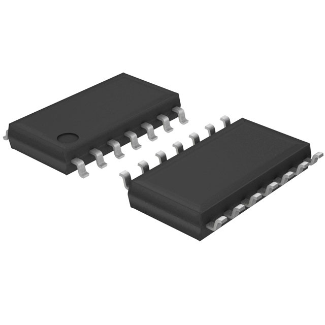
SN74HC266NSR

Why Choose Us?
Professional Platform
B2B & B2C purchasingDelivery at full speed
1-2 days deliveryWide variety
Original manufacturers365 days guarantee
Responsible quality
.png)


Tech Specifications
SN74HC266NSR Description
SN74HC266NSR Description
The SN74HC266NSR is a high-performance, 4-channel XNOR gate logic IC designed for a wide range of digital applications. Manufactured by Texas Instruments, this surface-mount device belongs to the 74HC series, renowned for its robustness and reliability. The SN74HC266NSR features a maximum propagation delay of 23ns at 6V and 50pF, ensuring fast and efficient signal processing. It operates within a supply voltage range of 2V to 6V, making it versatile for various power requirements.
This IC is equipped with open-drain outputs, providing flexibility in circuit design and enabling the use of pull-up resistors for level shifting and signal conditioning. The input logic levels are well-defined, with a low input range of 0.5V to 1.8V and a high input range of 1.5V to 4.2V, ensuring compatibility with a broad spectrum of digital systems. The SN74HC266NSR also boasts a maximum quiescent current of just 2 µA, contributing to low power consumption and making it suitable for battery-powered and energy-efficient applications.
SN74HC266NSR Features
- Logic Type: XNOR (Exclusive NOR) with 4 channels and 2 inputs per channel, providing versatile digital logic functionality.
- Mounting Type: Surface Mount, ideal for compact and high-density PCB designs.
- Package: Tape & Reel (TR), ensuring ease of handling and integration in automated assembly processes.
- Supply Voltage Range: 2V to 6V, offering flexibility in power supply options.
- Propagation Delay: Maximum of 23ns at 6V and 50pF, ensuring rapid signal processing and minimal latency.
- Input Logic Levels: Clearly defined low (0.5V to 1.8V) and high (1.5V to 4.2V) levels for reliable operation.
- Open Drain Outputs: Facilitates the use of pull-up resistors, enabling level shifting and signal conditioning.
- Low Quiescent Current: Maximum of 2 µA, contributing to energy efficiency and suitability for low-power applications.
- Compliance: REACH Unaffected and ROHS3 Compliant, ensuring environmental and regulatory compliance.
- Moisture Sensitivity Level (MSL): 1 (Unlimited), indicating robustness against moisture and suitability for various environmental conditions.
SN74HC266NSR Applications
The SN74HC266NSR is ideal for a variety of applications where high-speed, low-power digital logic is required. Its XNOR functionality makes it particularly useful in digital signal processing, error detection, and data synchronization tasks. Some specific use cases include:
- Digital Signal Processing: Utilizing the XNOR logic for phase detection and signal comparison in digital circuits.
- Error Detection: Implementing parity check circuits to detect errors in data transmission and storage.
- Data Synchronization: Aligning data streams in communication systems and digital interfaces.
- Battery-Powered Devices: Leveraging its low quiescent current to extend battery life in portable and handheld devices.
- Automotive and Industrial Electronics: Benefiting from its robustness and surface-mount design for compact and reliable systems.
Conclusion of SN74HC266NSR
The SN74HC266NSR is a versatile and high-performance XNOR gate logic IC that stands out due to its fast propagation delay, low power consumption, and flexible input logic levels. Its open-drain outputs and surface-mount design make it suitable for a wide range of applications, from digital signal processing to error detection and data synchronization. With its compliance to environmental and regulatory standards, the SN74HC266NSR is an excellent choice for modern electronic designs, offering reliability and efficiency in various digital systems.
FAQ
| Quantity | Unit Price | Ext. Price |
|---|---|---|
| 1+ | $0.58960 | $0.59 |
| 10+ | $0.41976 | $4.20 |
| 25+ | $0.37699 | $9.42 |
| 100+ | $0.32938 | $32.94 |
| 250+ | $0.30680 | $76.70 |
Not available to buy online? Want the lower wholesale price? Please Send RFQ to get best price, we will respond immediately


.png?x-oss-process=image/format,webp/resize,h_32)


