
 German
 Japanese
 Portuguese
 Korea
Korea
 Mexico
 Dutch
Dutch


Texas Instruments
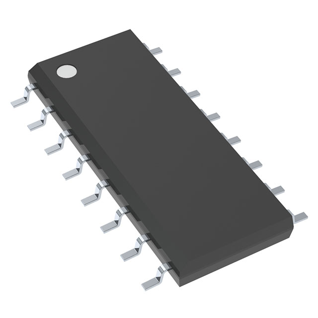
SN74LS279ADR

Why Choose Us?
Professional Platform
B2B & B2C purchasingDelivery at full speed
1-2 days deliveryWide variety
Original manufacturers365 days guarantee
Responsible quality
.png)


Tech Specifications
SN74LS279ADR Description
SN74LS279ADR Description
The SN74LS279ADR from Texas Instruments is a quad S-R (Set-Reset) latch integrated circuit housed in a 16-pin SOIC package, designed for surface-mount applications. Operating within a 4.75V to 5.25V supply range, this device is part of the 74LS series, known for its low-power Schottky (LS) technology. It features four independent 1:1 latches, each with standard TTL outputs, making it suitable for digital logic systems requiring stable state retention. With a propagation delay of 12ns and output current capabilities of 400µA (high) and 8mA (low), it balances speed and power efficiency. The device is RoHS3 compliant, REACH unaffected, and rated for operating temperatures from 0°C to 70°C, ensuring reliability in industrial and commercial environments.
SN74LS279ADR Features
- Quad S-R Latches: Four independent latches in a single package, reducing board space and complexity.
- Low-Power Schottky (LS) Technology: Combines high speed with reduced power consumption compared to standard TTL.
- Wide Operating Voltage (4.75V–5.25V): Compatible with standard 5V logic systems.
- Fast Propagation Delay (12ns): Ensures quick response in time-critical applications.
- High Output Drive (8mA sink current): Capable of driving multiple loads without external buffers.
- Surface-Mount (SOIC-16) Package: Ideal for compact, high-density PCB designs.
- Robust Compliance: Meets RoHS3, REACH, and EAR99 standards for global deployment.
SN74LS279ADR Applications
- Data Storage Systems: Used in registers and temporary storage for microprocessors or FPGAs.
- Control Logic Circuits: Ideal for debouncing switches or stabilizing control signals in industrial automation.
- Communication Equipment: Ensures signal integrity in buffering and routing applications.
- Consumer Electronics: Found in devices requiring state retention, such as gaming consoles or smart home systems.
- Automotive and Industrial Systems: Reliable performance in harsh environments due to its wide temperature range and robust construction.
Conclusion of SN74LS279ADR
The SN74LS279ADR is a versatile, high-performance quad S-R latch that excels in digital logic applications demanding low power, fast response, and compact design. Its four independent latches, LS technology, and compliance with industry standards make it a preferred choice for engineers designing data storage, control systems, and communication devices. Whether for consumer electronics or industrial automation, this IC delivers reliability and efficiency in a surface-mount form factor.
FAQ
| Quantity | Unit Price | Ext. Price |
|---|---|---|
| 1+ | $1.25840 | $1.26 |
| 10+ | $0.91960 | $9.20 |
| 25+ | $0.83424 | $20.86 |
| 100+ | $0.73999 | $74.00 |
| 250+ | $0.69506 | $173.77 |
Not available to buy online? Want the lower wholesale price? Please Send RFQ to get best price, we will respond immediately


.png?x-oss-process=image/format,webp/resize,h_32)


