
 German
 Japanese
 Portuguese
 Korea
Korea
 Mexico
 Dutch
Dutch


Texas Instruments
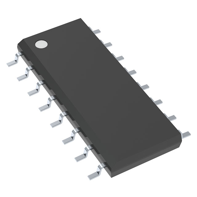
SN74LV4053ATDRQ1

Why Choose Us?
Professional Platform
B2B & B2C purchasingDelivery at full speed
1-2 days deliveryWide variety
Original manufacturers365 days guarantee
Responsible quality
.png)


Tech Specifications
SN74LV4053ATDRQ1 Description
The SN74LV4053ATDRQ1 is a high-performance, 16-channel analog multiplexer/switch from Texas Instruments. It is designed to efficiently route signals between multiple input channels and a single output channel, making it ideal for a wide range of applications.
Description:
The SN74LV4053ATDRQ1 is a member of Texas Instruments' 74LV family of logic devices. It is a 16-input, single-output multiplexer/switch that operates with low voltage supplies (1.2V to 3.6V) and offers high-speed performance. The device is available in a compact QFN package, making it suitable for space-constrained applications.
Features:
- 16 single-pole, single-throw (SPST) analog switches
- Single 4-bit digital control input for selecting the input channel
- Low on-resistance (50 ohms typical, max 100 ohms) for low signal loss
- 3-state outputs for easy cascading with other multiplexers or logic devices
- Wide operating voltage range (1.2V to 3.6V)
- High-speed performance (75MHz typical bandwidth)
- Low power consumption (6.2mA max at 3.3V supply)
- Short-circuit protection on all switch channels
- Guaranteed 2.5V tolerant inputs and outputs
- Available in a 24-pin QFN package
Applications:
- Medical equipment: Routing signals from multiple sensors to a single data acquisition system.
- Industrial control systems: Switching between various analog input channels for monitoring and control.
- Test and measurement equipment: Automating the testing of multiple input channels.
- Audio/Video applications: Routing audio or video signals between multiple sources and a single output device.
- Sensor interfaces: Multiplexing signals from various sensors for data acquisition and processing.
- Communication systems: Routing signals between multiple input channels and a single ADC or DAC.
- Battery monitoring systems: Measuring voltage levels from multiple battery cells.
The SN74LV4053ATDRQ1 is a versatile and high-performance multiplexer/switch that can be used in various applications where signal routing and channel selection are required. Its low power consumption, high-speed performance, and wide operating voltage range make it suitable for a wide range of applications, from medical equipment to industrial control systems.
FAQ
Not available to buy online? Want the lower wholesale price? Please Send RFQ to get best price, we will respond immediately


.png?x-oss-process=image/format,webp/resize,h_32)


