

Texas Instruments
SN74LV574ADWR
Flip Flops

Not available to buy online? Want the lower wholesale price? Please Send RFQ to get best price, we will respond immediately


.png?x-oss-process=image/format,webp/resize,p_30)


SN74LV574ADWR Description
SN74LV574ADWR Description
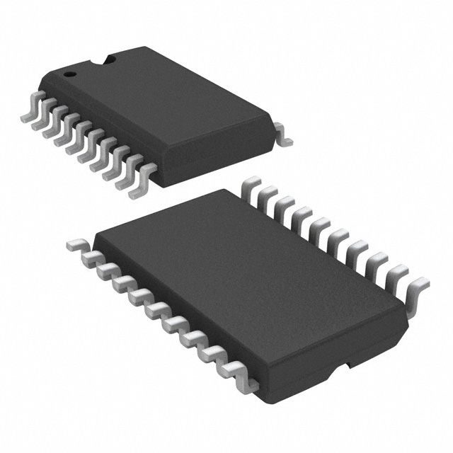
The SN74LV574ADWR from Texas Instruments is a high-performance, 8-bit D-type flip-flop designed for edge-triggered data storage applications. This surface-mount IC operates within a 2V to 5.5V supply range, making it compatible with both 3.3V and 5V systems. With a 175 MHz clock frequency and a max propagation delay of 10.6ns @ 5V, 50pF, it ensures reliable high-speed data transfer. The device features positive-edge triggering, 16mA output drive capability, and a low quiescent current of 20 µA, optimizing power efficiency. Packaged in a 20-SOIC (DWR) tape & reel format, it is RoHS3 compliant and suitable for automated assembly processes.
SN74LV574ADWR Features
- High-Speed Operation: Supports 175 MHz clock frequency for rapid data handling.
- Wide Voltage Range: 2V to 5.5V compatibility enhances design flexibility.
- Low Power Consumption: 20 µA quiescent current minimizes energy usage in idle states.
- Balanced Output Drive: 16mA source/sink current ensures robust signal integrity.
- Low Input Capacitance: 1.8 pF reduces loading effects on preceding stages.
- Industrial Robustness: MSL 1 (Unlimited) moisture sensitivity and REACH unaffected status ensure reliability.
- Space-Efficient Packaging: 20-SOIC footprint suits high-density PCB layouts.
SN74LV574ADWR Applications
- Data Buffering: Ideal for register banks and temporary storage in microprocessors.
- Bus Interface: Ensures stable signal transmission in I/O expansion circuits.
- Clock Domain Crossing: Mitigates metastability in multi-clock systems.
- Low-Power Systems: Suitable for battery-operated devices due to minimal Iq.
- Automotive & Industrial: Withstands harsh environments in control systems and sensor interfaces.
Conclusion of SN74LV574ADWR
The SN74LV574ADWR stands out for its speed, power efficiency, and versatility, making it a top choice for digital logic designs. Its wide voltage range and high drive strength cater to diverse applications, from embedded systems to automotive electronics. Texas Instruments’ reputation for quality ensures this flip-flop delivers long-term reliability, solidifying its position as a go-to solution for high-performance edge-triggered storage.
Tech Specifications
SN74LV574ADWR Documents
Download datasheets and manufacturer documentation for SN74LV574ADWR
Mult Dev 21/Dec/2022 SN54LV574A, SN74LV574A SN54LV574A, SN74LV574A Related Parts


Shopping Guide


.png?x-oss-process=image/format,webp/resize,h_32)


©2025 ERSA Electronics Corporation.