

Texas Instruments
SN74LVC00ADBRG4
Gates and Inverters

Not available to buy online? Want the lower wholesale price? Please Send RFQ to get best price, we will respond immediately


.png?x-oss-process=image/format,webp/resize,p_30)


SN74LVC00ADBRG4 Description
SN74LVC00ADBRG4 Description
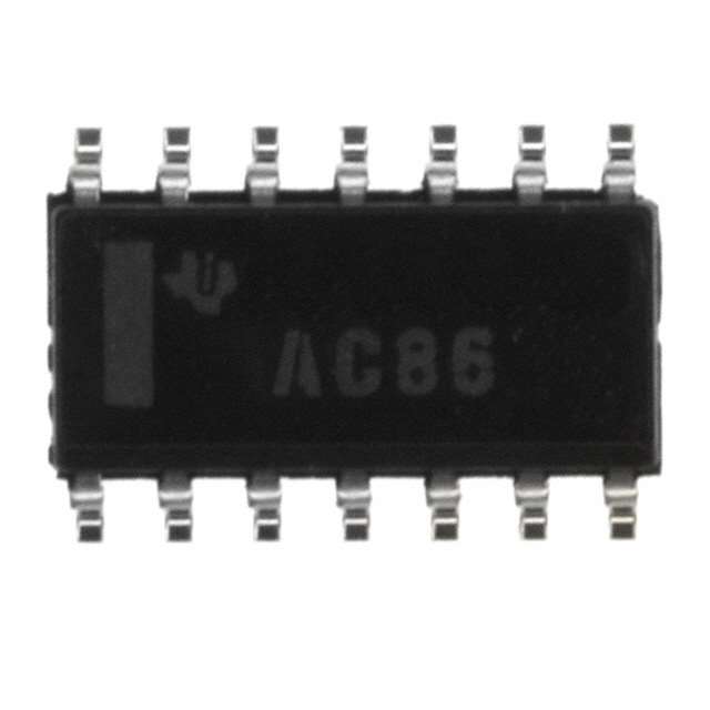
The SN74LVC00ADBRG4 is a high-performance, quad 2-input NAND gate IC from Texas Instruments, designed for a wide range of digital logic applications. This device is part of the 74LVC series, known for its excellent performance and reliability. The SN74LVC00ADBRG4 features a maximum propagation delay of 4.1ns at 3.3V with a load capacitance of 50pF, ensuring fast signal processing and high-speed operation. It operates within a supply voltage range of 1.65V to 3.6V, making it suitable for various power supply configurations. The input logic levels are specified as 0.7V to 0.8V for low and 1.7V to 2V for high, providing precise and reliable signal detection.
SN74LVC00ADBRG4 Features
- Logic Type: NAND Gate
- Number of Circuits: 4
- Number of Inputs per Circuit: 2
- Max Propagation Delay: 4.1ns @ 3.3V, 50pF
- Supply Voltage Range: 1.65V to 3.6V
- Input Logic Levels:
- Low: 0.7V to 0.8V
- High: 1.7V to 2V
- Current Specifications:
- Quiescent (Max): 1 µA
- Output High: 24mA
- Output Low: 24mA
- Mounting Type: Surface Mount
- Package: Tape & Reel (TR)
- Moisture Sensitivity Level (MSL): 1 (Unlimited)
- Compliance:
- REACH Status: REACH Unaffected
- RoHS Status: ROHS3 Compliant
- Harmonized Tariff Schedule (HTSUS): 8542.39.0001
SN74LVC00ADBRG4 Applications
The SN74LVC00ADBRG4 is ideal for applications requiring high-speed digital signal processing and logic operations. Its low propagation delay and wide supply voltage range make it suitable for a variety of electronic systems, including:
- Digital Signal Processing: Efficiently processes digital signals in high-speed communication systems.
- Microcontroller Interfaces: Provides reliable logic functions for interfacing with microcontrollers and other digital devices.
- Memory Management: Used in memory control circuits to manage data flow and signal processing.
- Consumer Electronics: Ideal for applications in smartphones, tablets, and other consumer electronics where compact size and high performance are critical.
Conclusion of SN74LVC00ADBRG4
The SN74LVC00ADBRG4 from Texas Instruments is a versatile and high-performance NAND gate IC that offers significant advantages over similar models. Its low propagation delay, wide supply voltage range, and precise input logic levels ensure reliable and efficient operation in various digital logic applications. The device's compliance with industry standards such as REACH and RoHS3 further enhances its suitability for modern electronic designs. Whether used in digital signal processing, microcontroller interfaces, or consumer electronics, the SN74LVC00ADBRG4 provides a robust and reliable solution for engineers and designers.
Tech Specifications
SN74LVC00ADBRG4 Documents
Download datasheets and manufacturer documentation for SN74LVC00ADBRG4
Mechanical Outline Drawing Product Change Notification 2024-05-24 (PDF) Product Change Notification 2024-07-30 (PDF) Logic Guide (Rev. AB) Little Logic Guide 2018 (Rev. G) SN74LVC00A Behavioral SPICE Model Related Parts


Shopping Guide


.png?x-oss-process=image/format,webp/resize,h_32)


©2025 ERSA Electronics Corporation.