

Texas Instruments
SN74LVC04ANSRG4
Gates and Inverters

Not available to buy online? Want the lower wholesale price? Please Send RFQ to get best price, we will respond immediately


.png?x-oss-process=image/format,webp/resize,p_30)


SN74LVC04ANSRG4 Description
SN74LVC04ANSRG4 Description
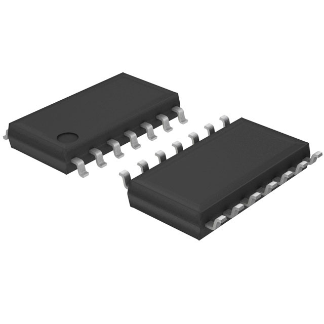
The SN74LVC04ANSRG4 is a high-performance inverter IC from Texas Instruments, featuring six independent inverter circuits. Each inverter has a single input and operates within a supply voltage range of 1.65V to 3.6V, making it suitable for a wide range of low-voltage applications. The device is designed for surface mount technology (SMT) and is packaged in a 14-pin small outline (SO) package, ensuring compact and reliable integration into modern electronic systems.
SN74LVC04ANSRG4 Features
- Low Propagation Delay: The SN74LVC04ANSRG4 boasts a maximum propagation delay of 4.3ns at 3.3V with a 50pF load, ensuring rapid signal inversion and minimal latency.
- Wide Operating Voltage Range: With a supply voltage range of 1.65V to 3.6V, this IC is versatile and can be used in various low-voltage systems.
- Low Quiescent Current: The maximum quiescent current is only 1 µA, making it ideal for low-power applications.
- High Output Current Capability: The device can source and sink up to 24mA, providing robust output drive capabilities.
- Moisture Sensitivity Level (MSL): Rated at MSL 1 (Unlimited), the SN74LVC04ANSRG4 is suitable for a wide range of manufacturing environments.
- Compliance and Standards: The IC is REACH unaffected and RoHS3 compliant, ensuring it meets environmental and safety standards.
- Input Logic Levels: The input logic levels are well-defined at 0.7V to 0.8V for low and 1.7V to 2V for high, ensuring reliable operation with various input signals.
SN74LVC04ANSRG4 Applications
The SN74LVC04ANSRG4 is ideal for applications requiring high-speed signal inversion and low power consumption. Its wide operating voltage range and robust output current capability make it suitable for a variety of electronic systems, including:
- Digital Signal Processing: Inverting digital signals in microcontroller and microprocessor systems.
- Communication Circuits: Inverting signals in data transmission and reception circuits.
- Consumer Electronics: Inverting signals in devices such as smartphones, tablets, and other portable electronics.
- Industrial Control Systems: Inverting control signals in automation and robotics applications.
Conclusion of SN74LVC04ANSRG4
The SN74LVC04ANSRG4 is a versatile and high-performance inverter IC that offers significant advantages over similar models. Its low propagation delay, wide operating voltage range, and low quiescent current make it an excellent choice for low-power, high-speed applications. The device's robust output current capability and compliance with environmental and safety standards further enhance its appeal. While the product is now obsolete, its technical specifications and performance benefits continue to make it a valuable component for existing systems and legacy designs.
Tech Specifications
SN74LVC04ANSRG4 Documents
Download datasheets and manufacturer documentation for SN74LVC04ANSRG4
SN54LVC04A, SN74LVC04A Carrier Tape Revision C 09/Apr/2015 Carrier Tape Revision B 30/Mar/2015 SN54LVC04A, SN74LVC04A Related Parts


Shopping Guide


.png?x-oss-process=image/format,webp/resize,h_32)


©2025 ERSA Electronics Corporation.