
 German
 Japanese
 Portuguese
 Korea
Korea
 Mexico
 Dutch
Dutch


Texas Instruments
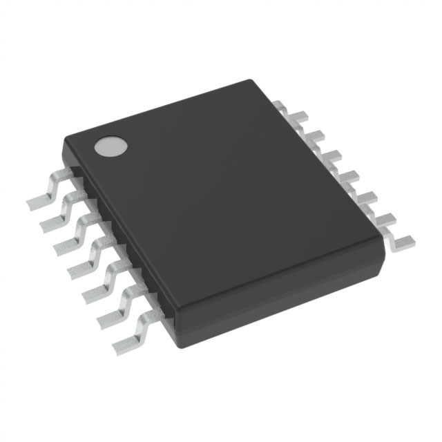
SN74LVC06APW

Why Choose Us?
Professional Platform
B2B & B2C purchasingDelivery at full speed
1-2 days deliveryWide variety
Original manufacturers365 days guarantee
Responsible quality
.png)


Tech Specifications
SN74LVC06APW Description
SN74LVC06APW Description
The SN74LVC06APW is a high-performance inverter logic IC chip manufactured by Texas Instruments. This device is part of the 74LVC series, known for its excellent performance and reliability in digital logic applications. The SN74LVC06APW features six inverters, each with a single input, making it suitable for a wide range of digital signal processing tasks.
Key technical specifications include a maximum propagation delay of 3.5 nanoseconds at 3.3V with a load capacitance of 50 picofarads. This low propagation delay ensures fast signal processing, making the SN74LVC06APW ideal for high-speed digital circuits. The device operates within a supply voltage range of 1.65V to 3.6V, providing flexibility in power supply requirements. Input logic levels are defined as 0.7V to 0.8V for low and 1.7V to 2V for high, ensuring compatibility with various digital systems.
The SN74LVC06APW is designed for surface-mount applications, packaged in a tube format, and features open-drain outputs. This allows for versatile circuit design and integration with other digital components. The device has a maximum quiescent current of 1 µA, contributing to low power consumption and energy efficiency. Additionally, the SN74LVC06APW is REACH unaffected and RoHS3 compliant, ensuring environmental safety and regulatory compliance.
SN74LVC06APW Features
- High-Speed Performance: With a maximum propagation delay of 3.5ns at 3.3V and 50pF, the SN74LVC06APW ensures rapid signal processing, making it suitable for high-speed digital applications.
- Wide Operating Voltage Range: The device operates within a supply voltage range of 1.65V to 3.6V, providing flexibility for various power supply configurations.
- Low Power Consumption: A maximum quiescent current of 1 µA ensures minimal power usage, making the SN74LVC06APW energy-efficient.
- Open-Drain Outputs: This feature allows for versatile circuit design and integration with other digital components, enhancing its usability in complex digital systems.
- Environmental Compliance: The SN74LVC06APW is REACH unaffected and RoHS3 compliant, ensuring it meets environmental safety and regulatory standards.
- Surface-Mount Compatibility: The device is designed for surface-mount applications, packaged in a tube format, making it easy to integrate into modern PCB designs.
SN74LVC06APW Applications
The SN74LVC06APW is ideal for a variety of digital signal processing applications, including:
- Digital Logic Circuits: The device's high-speed performance and low power consumption make it suitable for complex digital logic circuits.
- Data Processing: The six inverters with single inputs allow for efficient data processing and signal inversion in digital systems.
- Communication Systems: The SN74LVC06APW can be used in communication systems where fast signal processing and low power consumption are critical.
- Consumer Electronics: The device's versatility and compliance with environmental standards make it suitable for use in consumer electronics.
Conclusion of SN74LVC06APW
The SN74LVC06APW is a high-performance inverter logic IC chip that offers a combination of speed, flexibility, and environmental compliance. Its low propagation delay and wide operating voltage range make it suitable for high-speed digital applications, while its low power consumption and open-drain outputs enhance its versatility. The device's compliance with REACH and RoHS3 standards ensures it meets environmental safety and regulatory requirements. Overall, the SN74LVC06APW is an excellent choice for digital signal processing tasks in a variety of applications, from complex digital circuits to consumer electronics.
FAQ
| Quantity | Unit Price | Ext. Price |
|---|---|---|
| 1+ | $0.87120 | $0.87 |
| 10+ | $0.62480 | $6.25 |
| 90+ | $0.50082 | $45.07 |
| 180+ | $0.47505 | $85.51 |
| 270+ | $0.46217 | $124.79 |
Not available to buy online? Want the lower wholesale price? Please Send RFQ to get best price, we will respond immediately


.png?x-oss-process=image/format,webp/resize,h_32)


