
 German
 Japanese
 Portuguese
 Korea
Korea
 Mexico
 Dutch
Dutch


Texas Instruments
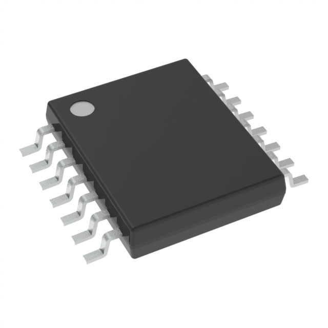
SN74LVC06APWR

Why Choose Us?
Professional Platform
B2B & B2C purchasingDelivery at full speed
1-2 days deliveryWide variety
Original manufacturers365 days guarantee
Responsible quality
.png)


Tech Specifications
SN74LVC06APWR Description
The SN74LVC06APWR is a hex inverter buffer/driver integrated circuit (IC) manufactured by Texas Instruments. It is a member of the 74LVC06 series, which are high-speed Si-gate CMOS devices designed for low-power applications. Here's a brief description, features, and applications of the SN74LVC06APWR:
Description:
The SN74LVC06APWR is a hex inverter buffer/driver IC that consists of six independent inverting buffers. It is designed to provide a high-voltage output from a low-voltage input, making it suitable for interfacing between systems with different voltage levels. The device is available in a PowerSO-20 package.
Features:
- High-voltage tolerant input and output: The SN74LVC06APWR can handle input voltages up to 5.5V and output voltages up to 5.5V, making it suitable for interfacing with systems operating at different voltage levels.
- Low-power operation: The device is designed for low-power applications, with a typical supply current of 5mA.
- High-speed performance: The SN74LVC06APWR offers fast switching speeds, with a typical propagation delay of 3.5ns.
- Wide operating temperature range: The device can operate in a wide temperature range of -40°C to 125°C, making it suitable for industrial and automotive applications.
- High noise immunity: The IC provides high noise immunity, ensuring reliable operation in noisy environments.
- CMOS technology: The device is built using silicon-gate CMOS technology, which offers advantages such as low power consumption, high noise immunity, and compatibility with TTL and CMOS systems.
Applications:
- Voltage level translation: The SN74LVC06APWR can be used to interface between systems with different voltage levels, such as converting a low-voltage signal to a higher voltage level or vice versa.
- Buffering and signal conditioning: The hex inverter buffer/driver can be used to buffer and condition signals in digital systems, improving signal integrity and reducing signal degradation due to long transmission lines or high-load capacitance.
- Digital signal processing: The device can be used in digital signal processing applications, such as filtering, waveform generation, and signal modulation.
- Industrial control systems: The wide operating temperature range and high noise immunity make the SN74LVC06APWR suitable for use in industrial control systems, where reliable operation in harsh environments is crucial.
- Automotive applications: The device's high-voltage tolerance and wide operating temperature range make it suitable for automotive applications, such as engine control units, infotainment systems, and safety systems.
- Consumer electronics: The SN74LVC06APWR can be used in various consumer electronics applications, such as smartphones, tablets, and smart home devices, for signal buffering and voltage level translation.
In summary, the SN74LVC06APWR is a versatile hex inverter buffer/driver IC that offers high-voltage tolerance, low-power operation, and high-speed performance. It is suitable for a wide range of applications, including voltage level translation, buffering, signal conditioning, digital signal processing, and interfacing in industrial control systems, automotive applications, and consumer electronics.
FAQ
| Quantity | Unit Price | Ext. Price |
|---|---|---|
| 5+ | $0.29215 | $1.46 |
| 50+ | $0.23752 | $11.88 |
| 150+ | $0.21084 | $31.63 |
| 500+ | $0.18704 | $93.52 |
Not available to buy online? Want the lower wholesale price? Please Send RFQ to get best price, we will respond immediately


.png?x-oss-process=image/format,webp/resize,h_32)


