

Texas Instruments
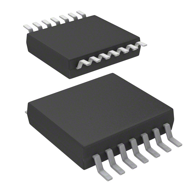
SN74LVC07ADGVR
Buffers, Drivers, Receivers, Transceivers

Not available to buy online? Want the lower wholesale price? Please Send RFQ to get best price, we will respond immediately


.png?x-oss-process=image/format,webp/resize,p_30)


SN74LVC07ADGVR Description
SN74LVC07ADGVR Description
The SN74LVC07ADGVR is a high-performance buffer from Texas Instruments, specifically designed to provide reliable signal conditioning in various electronic systems. This device is part of the 74LVC series, known for its low-voltage operation and high-speed performance. With a supply voltage range of 1.65V to 5.5V, it is well-suited for low-power applications. The SN74LVC07ADGVR is an open-drain output type, which allows for flexible integration into different circuit designs.
SN74LVC07ADGVR Features
-
Technical Specifications: The SN74LVC07ADGVR operates with a single bit per element and features six elements, making it versatile for multiplexing and signal buffering tasks. It is designed for surface mount applications, which allows for compact and efficient board layouts. The device is compliant with the RoHS3 directive, indicating its commitment to environmental standards. Moreover, it is classified under the EAR99 category, facilitating international trade without export controls.
-
Performance Benefits: The SN74LVC07ADGVR boasts a wide supply voltage range, which makes it adaptable to various power supply conditions. Its open-drain output configuration offers design flexibility, especially in applications requiring pull-up resistors. The device's unlimited moisture sensitivity level (MSL 1) ensures reliable performance across a broad range of environmental conditions.
-
Unique Features and Advantages: Compared to similar models, the SN74LVC07ADGVR stands out with its robust design, ensuring consistent performance even in challenging environments. The wide operating voltage range and open-drain output make it an ideal choice for applications requiring a flexible and reliable signal buffer.
SN74LVC07ADGVR Applications
-
Communication Systems: The SN74LVC07ADGVR is ideal for buffering signals in communication systems, such as routers and switches, where signal integrity and low power consumption are critical.
-
Automotive Electronics: In automotive applications, this buffer can be used to ensure signal reliability in infotainment systems, sensor interfaces, and control units.
-
Industrial Control Systems: The device's robustness and wide voltage range make it suitable for buffering signals in industrial control systems, where reliability and performance are paramount.
Conclusion of SN74LVC07ADGVR
The SN74LVC07ADGVR is a versatile and reliable buffer IC from Texas Instruments, designed to meet the demanding requirements of modern electronic systems. Its unique combination of low-voltage operation, open-drain output, and environmental resilience make it an excellent choice for a wide range of applications, from communication systems to automotive electronics. With its performance benefits and adherence to industry standards, the SN74LVC07ADGVR is a trusted component for ensuring signal integrity in various electronic designs.
Tech Specifications
SN74LVC07ADGVR Documents
Download datasheets and manufacturer documentation for SN74LVC07ADGVR
SN74LVC07A SN74LVC07A Datsheet Update 05/Jun/2015 Related Parts


Shopping Guide


.png?x-oss-process=image/format,webp/resize,h_32)


©2025 ERSA Electronics Corporation.