
 German
 Japanese
 Portuguese
 Korea
Korea
 Mexico
 Dutch
Dutch


Texas Instruments
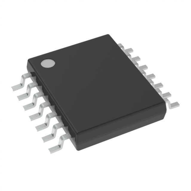
SN74LVC07APWT

Why Choose Us?
Professional Platform
B2B & B2C purchasingDelivery at full speed
1-2 days deliveryWide variety
Original manufacturers365 days guarantee
Responsible quality
.png)


Tech Specifications
SN74LVC07APWT Description
The Texas Instruments SN74LVC07APWT is a high-performance, low-voltage, low-power logic gate that is part of the 74LVCxx family of devices. It is designed to provide high-speed operation with low power consumption, making it ideal for a wide range of applications.
Description:
The SN74LVC07APWT is a quad 2-input AND gate, which means it has four separate AND gates, each with two inputs. The device is available in a small-outline, wide-body package (SO-16W) and operates over a wide supply voltage range of 2.0V to 5.5V.
Features:
- High-speed operation: The SN74LVC07APWT offers fast switching speeds, with a typical propagation delay of 3.5 ns.
- Low power consumption: The device has a low quiescent current of 2.5 mA, making it suitable for battery-powered applications.
- Wide supply voltage range: The SN74LVC07APWT can operate over a supply voltage range of 2.0V to 5.5V, making it compatible with various power supply systems.
- High noise immunity: The device has a high input voltage range, which helps to minimize the effects of noise on its operation.
- Low output voltage: The SN74LVC07APWT has a low output voltage, which helps to reduce power dissipation in the system.
Applications:
The SN74LVC07APWT is suitable for a wide range of applications, including:
- Digital signal processing: The high-speed operation and low power consumption make it ideal for use in digital signal processing applications.
- Power management: The device can be used in power management circuits to control the flow of power to various components in a system.
- Communication systems: The SN74LVC07APWT can be used in communication systems, such as routers and switches, to process and route digital signals.
- Automotive electronics: The device's low power consumption and wide supply voltage range make it suitable for use in automotive electronics, such as infotainment systems and engine control units.
- Industrial control systems: The SN74LVC07APWT can be used in industrial control systems to process and control digital signals in various applications, such as motor control and sensor interfacing.
In summary, the Texas Instruments SN74LVC07APWT is a versatile, high-speed, low-power quad 2-input AND gate that offers a wide range of features and applications. Its high-speed operation, low power consumption, and wide supply voltage range make it an ideal choice for various digital signal processing, power management, communication, automotive, and industrial control applications.
FAQ
| Quantity | Unit Price | Ext. Price |
|---|---|---|
| 1+ | $0.85360 | $0.85 |
| 10+ | $0.61072 | $6.11 |
| 25+ | $0.55123 | $13.78 |
| 100+ | $0.48523 | $48.52 |
| 250+ | $0.45380 | $113.45 |
Not available to buy online? Want the lower wholesale price? Please Send RFQ to get best price, we will respond immediately


.png?x-oss-process=image/format,webp/resize,h_32)


