
Texas Instruments
SN74LVC08APW
Gates and Inverters


.png?x-oss-process=image/format,webp/resize,p_30)


SN74LVC08APW Description
SN74LVC08APW Description
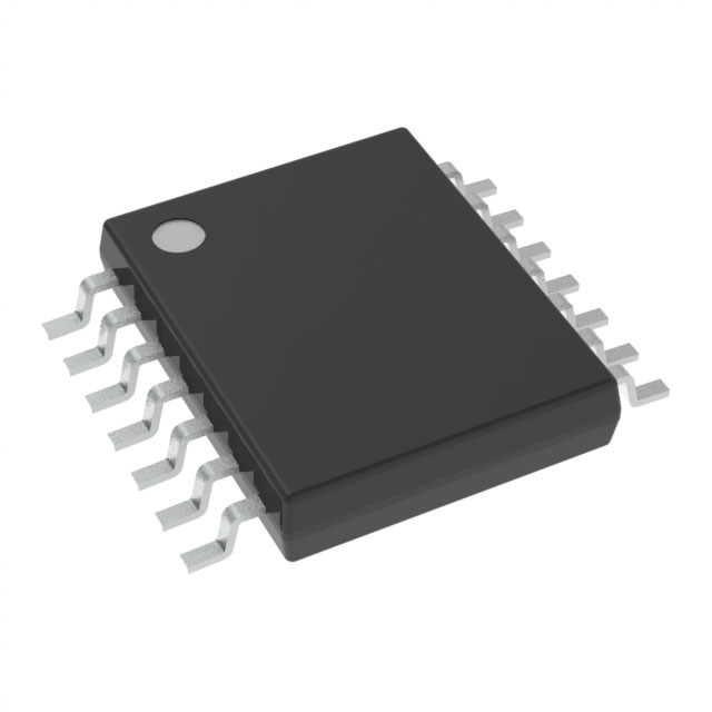
The SN74LVC08APW is a high-performance, dual 2-input AND gate from Texas Instruments, part of the 74LVC series. This surface-mount IC operates within a supply voltage range of 1.65V to 3.6V and boasts a maximum propagation delay of 3.9ns at 3.3V and 50pF. It is designed to meet the requirements of modern digital systems, offering low power consumption, high noise immunity, and excellent performance.
SN74LVC08APW Features
- Logic Type: AND Gate, providing reliable logical operations in digital circuits.
- Max Propagation Delay: 3.9ns @ 3.3V, 50pF, ensuring fast signal processing.
- Voltage - Supply: 1.65V ~ 3.6V, supporting a wide range of power supply options.
- Input Logic Levels: Low (0.7V ~ 0.8V) and High (1.7V ~ 2V), ensuring accurate signal detection.
- Current - Quiescent (Max): 1 µA, contributing to low power consumption in standby mode.
- Current - Output High, Low: 24mA, 24mA, providing sufficient drive capability for downstream devices.
- Mounting Type: Surface Mount, facilitating integration into compact electronic designs.
- RoHS Status: ROHS3 Compliant, adhering to environmental regulations.
- Moisture Sensitivity Level (MSL): 1 (Unlimited), indicating robustness against moisture.
SN74LVC08APW Applications
The SN74LVC08APW is ideal for a variety of applications where high-speed, low-power digital logic is required:
- Automotive Electronics: For control systems and sensor interfaces that demand rapid signal processing and low power consumption.
- Industrial Control Systems: In environments where noise immunity and reliable operation are critical.
- Telecommunications: For signal processing in base stations and switching equipment.
- Consumer Electronics: In devices where space is at a premium, such as smartphones and tablets.
Conclusion of SN74LVC08APW
The SN74LVC08APW stands out for its combination of high-speed performance, low power consumption, and robust design, making it an excellent choice for demanding digital applications. Its wide supply voltage range, low quiescent current, and compliance with environmental standards further enhance its appeal in the electronics industry. With its versatility and reliability, the SN74LVC08APW is a valuable component for designers looking to optimize their digital systems.
Tech Specifications
SN74LVC08APW Documents
Download datasheets and manufacturer documentation for SN74LVC08APW
 SN54LVC08A, SN74LVC08A
  Reels 19/Apr/2018 Reel 10/Jul/2018
  SN54LVC08A, SN74LVC08A
  Design 22/Feb/2022
 Shopping Guide


.png?x-oss-process=image/format,webp/resize,h_32)


