

Texas Instruments
SN74LVC112ADR
Flip Flops

Not available to buy online? Want the lower wholesale price? Please Send RFQ to get best price, we will respond immediately


.png?x-oss-process=image/format,webp/resize,p_30)


SN74LVC112ADR Description
SN74LVC112ADR Description
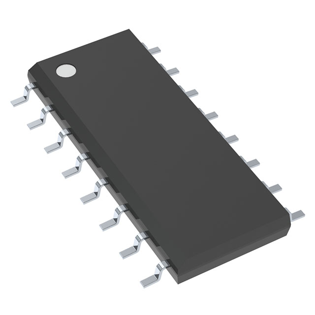
The SN74LVC112ADR is a dual JK-type flip-flop integrated circuit (IC) designed for high-performance digital applications. Manufactured by Texas Instruments, this IC is part of the 74LVC series, known for its robustness and reliability in various electronic systems. The SN74LVC112ADR features a clock frequency of up to 150 MHz, ensuring rapid data processing and synchronization. It operates within a supply voltage range of 1.65V to 3.6V, providing flexibility for different power supply configurations.
This IC is designed with a complementary output type, triggered on the negative edge, making it suitable for applications requiring precise timing control. Each flip-flop element in the SN74LVC112ADR is capable of handling 1 bit of data, and the device includes set (preset) and reset functions for enhanced control over data storage and manipulation. The IC is packaged in a 16-pin SOIC (Small Outline Integrated Circuit) format, ideal for surface mount applications.
SN74LVC112ADR Features
- High-Speed Operation: With a maximum clock frequency of 150 MHz, the SN74LVC112ADR ensures efficient data handling and synchronization in high-speed digital systems.
- Low Power Consumption: The IC operates within a supply voltage range of 1.65V to 3.6V, and features a quiescent current of only 10 µA, making it suitable for low-power applications.
- Complementary Outputs: The complementary output type provides flexibility in circuit design, allowing for both positive and negative logic levels.
- Negative Edge Triggering: This feature ensures precise timing control, making the IC ideal for applications requiring accurate data capture and processing.
- Set and Reset Functions: The inclusion of set (preset) and reset functions allows for enhanced control over the flip-flop's state, facilitating reliable data storage and manipulation.
- Robust Performance: The SN74LVC112ADR is designed to withstand a maximum propagation delay of 5.9ns at 3.3V and 50pF, ensuring reliable performance even under demanding conditions.
- Compliance and Reliability: The IC is REACH unaffected and RoHS3 compliant, ensuring environmental safety and regulatory compliance. It also has a moisture sensitivity level (MSL) of 1, making it suitable for a wide range of manufacturing processes.
SN74LVC112ADR Applications
The SN74LVC112ADR is ideal for a variety of applications requiring high-speed, reliable data processing and synchronization. Some specific use cases include:
- Digital Signal Processing: The high clock frequency and precise timing control make the SN74LVC112ADR suitable for applications involving digital signal processing, such as in communication systems and audio processing circuits.
- Data Storage and Manipulation: The set and reset functions, along with the complementary outputs, provide enhanced control over data storage and manipulation, making the IC ideal for use in memory circuits and data processing applications.
- Control Systems: The negative edge triggering and low power consumption make the SN74LVC112ADR suitable for use in control systems, where precise timing and energy efficiency are critical.
- Consumer Electronics: The compact 16-pin SOIC package and surface mount compatibility make the IC suitable for use in consumer electronics, where space and reliability are key considerations.
Conclusion of SN74LVC112ADR
The SN74LVC112ADR from Texas Instruments is a versatile and reliable dual JK-type flip-flop IC, offering high-speed operation, low power consumption, and precise timing control. Its complementary outputs, negative edge triggering, and set and reset functions provide enhanced control over data storage and manipulation, making it suitable for a wide range of applications. The IC's compliance with environmental and regulatory standards, along with its robust performance, ensures reliability and safety in various electronic systems. Whether used in digital signal processing, data storage, control systems, or consumer electronics, the SN74LVC112ADR is an excellent choice for engineers and designers seeking a high-performance, reliable solution.
Tech Specifications
SN74LVC112ADR Documents
Download datasheets and manufacturer documentation for SN74LVC112ADR
SN74LVC112A SN74LVC112A Mult Devices Font 21/Apr/2018 Related Parts


Shopping Guide


.png?x-oss-process=image/format,webp/resize,h_32)


©2025 ERSA Electronics Corporation.