
 German
 Japanese
 Portuguese
 Korea
Korea
 Mexico
 Dutch
Dutch


Texas Instruments
SN74LVC125APWG4

Why Choose Us?
Professional Platform
B2B & B2C purchasingDelivery at full speed
1-2 days deliveryWide variety
Original manufacturers365 days guarantee
Responsible quality
.png)


Tech Specifications
SN74LVC125APWG4 Description
SN74LVC125APWG4 Description
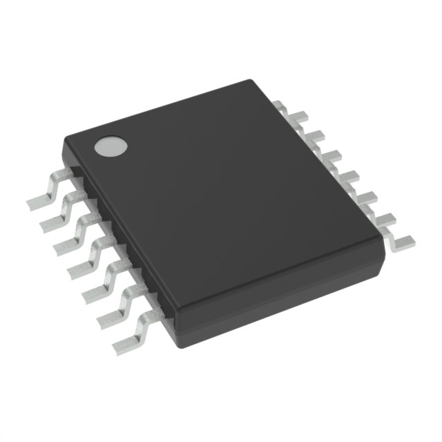
The SN74LVC125APWG4 is a high-performance, non-inverting buffer IC designed for a wide range of digital applications. Manufactured by Texas Instruments, this device is part of the 74LVC series, known for its low-voltage operation and high-speed performance. The SN74LVC125APWG4 features four independent non-inverting buffers, each capable of handling one bit of data. It operates within a supply voltage range of 1.65V to 3.6V, making it suitable for various power supply environments. The device is housed in a 14-TSSOP package, which is ideal for surface-mount applications, ensuring easy integration into compact and high-density PCB designs.
SN74LVC125APWG4 Features
The SN74LVC125APWG4 offers several key features that set it apart from similar models:
- Low-Voltage Operation: The ability to operate within a voltage range of 1.65V to 3.6V makes it versatile for modern low-power systems.
- High-Speed Performance: With a maximum operating frequency of up to 100 MHz, it ensures fast data transmission and processing.
- High Current Capability: Each buffer can drive up to 24mA in both high and low states, providing robust signal integrity.
- Surface-Mount Compatibility: The 14-TSSOP package is designed for surface-mount technology, facilitating easy installation and high-density board layouts.
- Compliance and Safety: It is REACH unaffected and RoHS3 compliant, ensuring environmental safety and regulatory adherence.
- Moisture Sensitivity Level: With an MSL rating of 1 (unlimited), it is suitable for storage and handling in various environments without additional moisture protection.
SN74LVC125APWG4 Applications
The SN74LVC125APWG4 is ideal for a variety of applications due to its robust performance and versatility:
- Digital Signal Buffering: It can be used to buffer digital signals in microcontroller and microprocessor systems, ensuring signal integrity over long traces.
- Bus Line Drivers: It is suitable for driving bus lines in computer systems, ensuring reliable data transmission across multiple devices.
- Memory Interface Applications: It can be used in memory modules to drive address and data lines, enhancing the overall system performance.
- Communication Systems: It can be employed in communication systems to buffer and drive control signals, ensuring reliable data transfer.
- Consumer Electronics: Given its low-voltage operation and compact size, it is well-suited for consumer electronics where space and power efficiency are critical.
Conclusion of SN74LVC125APWG4
The SN74LVC125APWG4 from Texas Instruments is a versatile and high-performance non-inverting buffer IC that offers significant advantages for modern digital systems. Its wide voltage range, high current capability, and compact surface-mount package make it an ideal choice for a variety of applications, from microcontroller interfacing to memory modules. With its compliance to environmental and safety standards, it ensures reliability and sustainability in design. Whether used in consumer electronics, communication systems, or industrial applications, the SN74LVC125APWG4 delivers robust performance and ease of integration, making it a standout choice in the logic IC market.
FAQ
Not available to buy online? Want the lower wholesale price? Please Send RFQ to get best price, we will respond immediately


.png?x-oss-process=image/format,webp/resize,h_32)


