

Texas Instruments
SN74LVC125ARGYR
Buffers, Drivers, Receivers, Transceivers

Not available to buy online? Want the lower wholesale price? Please Send RFQ to get best price, we will respond immediately


- 5+
- $0.28429
- $1.42
- 50+
- $0.23118
- $11.56
- 150+
- $0.20842
- $31.26
- 500+
- $0.18002
- $90.01

.png?x-oss-process=image/format,webp/resize,p_30)


SN74LVC125ARGYR Description
The SN74LVC125ARGYR is a high-speed quad 2-input OR gate integrated circuit (IC) manufactured by Texas Instruments. Here is a brief description of the model, its features, and applications:
Description:
The SN74LVC125ARGYR is a member of the 74LVC125 family of quad 2-input OR gates. It is a high-performance, low-power device that provides four independent OR gate functions in a single package. The device is designed to operate over a wide supply voltage range and offers excellent noise immunity and propagation delay characteristics.
Features:
- Quad 2-input OR gate functionality
- Wide supply voltage range: 2.0V to 6.0V
- High-speed performance with typical propagation delay of 3.3ns (maximum)
- Low power consumption: 1.2mA (typical) at a supply voltage of 5V
- Excellent noise immunity with a typical threshold voltage of 1.3V
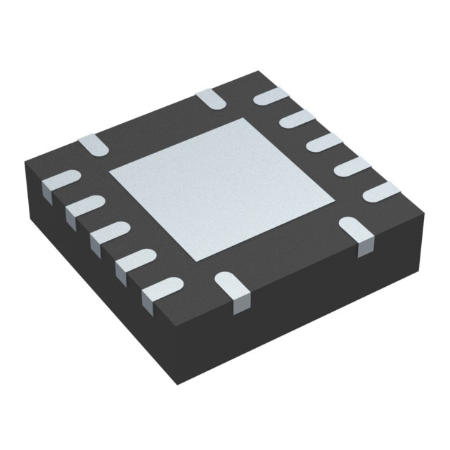
- 1.65mm pitch, 16-pin narrow body QFN package (ARGYR)
- RoHS-compliant and lead-free
- Industrial temperature range: -40°C to +85°C
Applications:
- Digital logic and control systems
- Signal conditioning and amplification
- Data acquisition and processing systems
- Telecommunication equipment
- Automotive control systems
- Industrial control and automation
- Battery monitoring and management systems
- High-speed data transmission and switching applications
The SN74LVC125ARGYR is a versatile and reliable solution for various digital logic applications, offering high-speed performance, low power consumption, and excellent noise immunity in a compact package.
Tech Specifications
SN74LVC125ARGYR Documents
Download datasheets and manufacturer documentation for SN74LVC125ARGYR
SN74LVC125A SN74LVC125A Related Parts


Shopping Guide


.png?x-oss-process=image/format,webp/resize,h_32)


©2025 ERSA Electronics Corporation.