
Texas Instruments
SN74LVC1G06DBVRG4
Gates and Inverters


.png?x-oss-process=image/format,webp/resize,p_30)


SN74LVC1G06DBVRG4 Description
SN74LVC1G06DBVRG4 Description
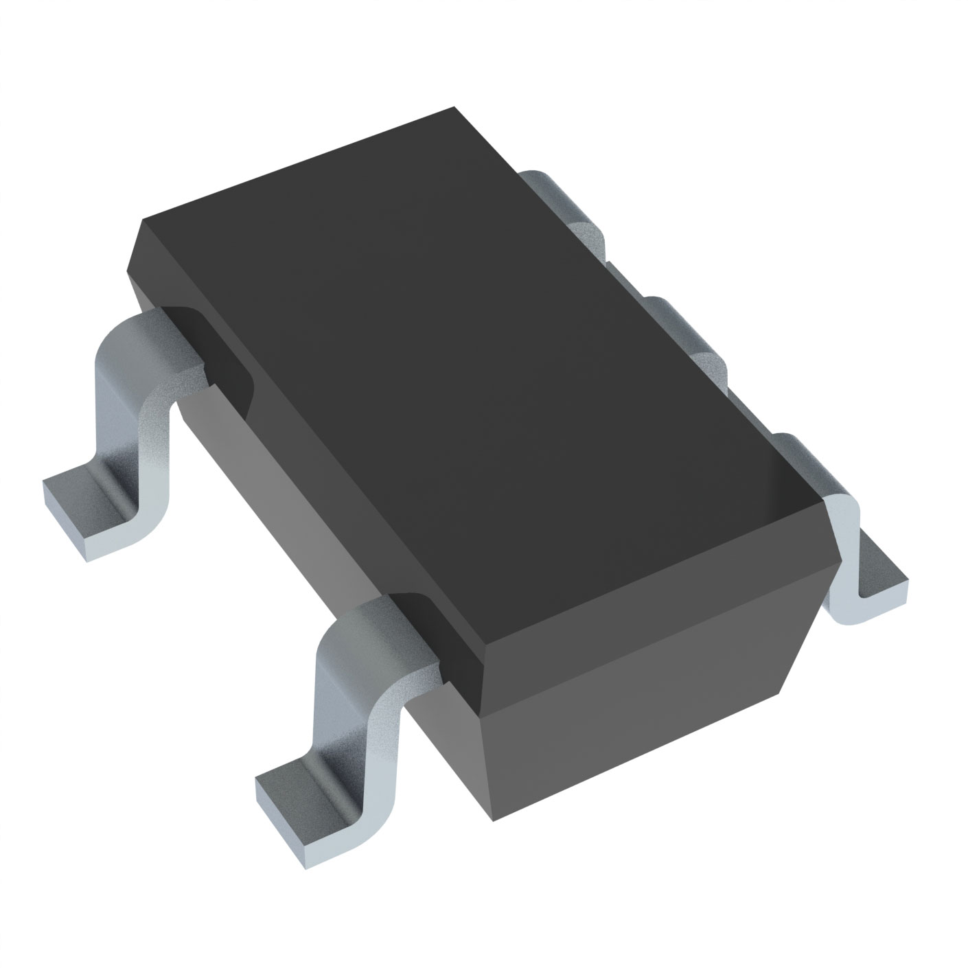
The SN74LVC1G06DBVRG4 is a high-performance inverter IC designed for a wide range of digital logic applications. Manufactured by Texas Instruments, this single-channel inverter belongs to the 74LVC series and is packaged in a compact SOT23-5 surface-mount package. It operates over a wide supply voltage range of 1.65V to 5.5V, making it suitable for various power supply configurations.
This inverter features an open-drain output, which allows for versatile circuit design and compatibility with different logic levels. The device has a maximum propagation delay of 3.5ns at 5V with a load capacitance of 50pF, ensuring fast signal inversion and minimal delay in high-speed applications. The input logic levels are well-defined, with a low input range of 0.58V to 1.65V and a high input range of 1.07V to 3.85V, providing robust and reliable operation.
SN74LVC1G06DBVRG4 Features
- Logic Type: Inverter
- Series: 74LVC
- Package: SOT23-5
- Mounting Type: Surface Mount
- Voltage - Supply: 1.65V to 5.5V
- Max Propagation Delay @ V, Max CL: 3.5ns @ 5V, 50pF
- Input Logic Level - Low: 0.58V to 1.65V
- Input Logic Level - High: 1.07V to 3.85V
- Current - Quiescent (Max): 10 µA
- Features: Open Drain
- Number of Inputs: 1
- Number of Circuits: 1
- Moisture Sensitivity Level (MSL): 1 (Unlimited)
- ECCN: EAR99
- HTSUS: 8542.39.0001
- REACH Status: REACH Unaffected
- RoHS Status: ROHS3 Compliant
SN74LVC1G06DBVRG4 Applications
The SN74LVC1G06DBVRG4 is ideal for applications requiring a compact, high-speed inverter with open-drain output. Its wide operating voltage range and low quiescent current make it suitable for battery-powered devices and other low-power applications. The open-drain feature allows for easy interfacing with various logic families and pull-up resistor configurations, enhancing its versatility.
Specific use cases include:
- Digital Signal Inversion: Ideal for inverting digital signals in communication interfaces, microcontroller peripherals, and digital circuits.
- Level Shifting: Can be used to shift logic levels between different voltage domains, ensuring compatibility between devices with varying supply voltages.
- Bus Control: The open-drain output is well-suited for bus control applications where multiple devices share a common bus line.
- Battery-Powered Devices: The low quiescent current and wide voltage range make it suitable for portable and battery-operated equipment.
Conclusion of SN74LVC1G06DBVRG4
The SN74LVC1G06DBVRG4 from Texas Instruments is a versatile and high-performance inverter IC that offers significant advantages over similar models. Its compact SOT23-5 package, wide operating voltage range, and open-drain output make it an excellent choice for a variety of digital logic applications. The low propagation delay and well-defined input logic levels ensure reliable and fast signal inversion, making it suitable for high-speed circuits.
With its RoHS3 compliance and REACH unaffected status, the SN74LVC1G06DBVRG4 meets the stringent environmental and regulatory requirements of the electronics industry. Its moisture sensitivity level of 1 (unlimited) ensures robustness and reliability in various environmental conditions.
Overall, the SN74LVC1G06DBVRG4 is a reliable and efficient solution for digital signal inversion and level shifting, making it a valuable component in modern electronic designs.
Tech Specifications
SN74LVC1G06DBVRG4 Documents
Download datasheets and manufacturer documentation for SN74LVC1G06DBVRG4
 Additional Assembly sites 21/Sep/2021
  SN74LVC1G06 Datasheet
  SN74LVC1G06 12/Jan/2018 Copper Wire Base 31/Mar/2014
 Shopping Guide


.png?x-oss-process=image/format,webp/resize,h_32)


