
Texas Instruments
SN74LVC1G07DCKTE4
Buffers, Drivers, Receivers, Transceivers


.png?x-oss-process=image/format,webp/resize,p_30)


SN74LVC1G07DCKTE4 Description
SN74LVC1G07DCKTE4 Description
The SN74LVC1G07DCKTE4 is a single non-inverting buffer designed by Texas Instruments, a leading manufacturer in the semiconductor industry. This logic IC chip is part of the 74LVC series, known for its high performance and reliability. The device features a single non-inverting buffer with open-drain output, making it suitable for a wide range of applications where signal buffering and level shifting are required. It operates within a voltage supply range of 1.65V to 5.5V, providing flexibility for various power supply configurations.
SN74LVC1G07DCKTE4 Features
- Single Non-Inverting Buffer: The SN74LVC1G07DCKTE4 is designed to provide a single non-inverting buffer, ensuring that the output signal maintains the same logic state as the input signal. This feature is crucial for applications requiring signal integrity and minimal signal distortion.
- Open-Drain Output: The open-drain output type allows for flexible circuit design, enabling the use of pull-up resistors to achieve desired voltage levels. This configuration is particularly useful in applications involving multiple devices sharing a common bus.
- Wide Voltage Range: The device operates within a voltage supply range of 1.65V to 5.5V, making it compatible with a variety of power supply configurations and ensuring robust performance across different operating conditions.
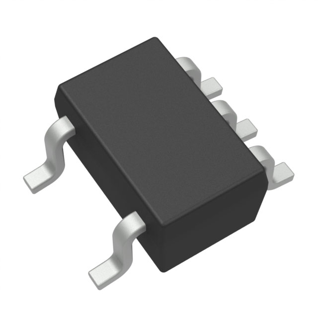
- Surface Mount Technology: The SN74LVC1G07DCKTE4 is available in a surface mount package, specifically the SC70-5 package. This mounting type is ideal for modern PCB designs, offering space-saving benefits and ease of integration into compact systems.
- Compliance and Reliability: The device is REACH unaffected and RoHS3 compliant, ensuring that it meets the highest environmental and safety standards. Additionally, it has a moisture sensitivity level (MSL) of 1 (unlimited), making it suitable for storage and handling in various environments without the risk of moisture-related damage.
- Packaging: The SN74LVC1G07DCKTE4 is packaged in tape and reel (TR), facilitating efficient handling and assembly processes in high-volume manufacturing environments.
SN74LVC1G07DCKTE4 Applications
The SN74LVC1G07DCKTE4 is ideal for a variety of applications due to its versatile design and performance characteristics. Some specific use cases include:
- Signal Buffering: The non-inverting buffer is perfect for applications where signal integrity needs to be maintained, such as in digital communication systems and data transmission lines.
- Level Shifting: The wide voltage range allows the device to be used in level-shifting applications, where it can convert signals between different voltage levels, ensuring compatibility between various components in a system.
- Bus Applications: The open-drain output makes the SN74LVC1G07DCKTE4 suitable for bus applications, where multiple devices share a common signal line. This feature enables efficient communication and reduces the complexity of the circuit design.
- Consumer Electronics: The compact SC70-5 package and surface mount technology make it ideal for consumer electronics, where space and ease of integration are critical factors.
- Industrial Control Systems: The robust performance and wide operating voltage range make it suitable for industrial control systems, where reliability and flexibility are paramount.
Conclusion of SN74LVC1G07DCKTE4
The SN74LVC1G07DCKTE4 from Texas Instruments is a versatile and reliable logic IC chip that offers significant benefits for a wide range of applications. Its single non-inverting buffer with open-drain output, wide voltage range, and surface mount packaging make it an ideal choice for signal buffering, level shifting, and bus applications. The device's compliance with environmental and safety standards, along with its moisture sensitivity level of 1 (unlimited), ensures that it is suitable for various operating conditions and manufacturing processes. Whether used in consumer electronics, industrial control systems, or other digital applications, the SN74LVC1G07DCKTE4 provides a robust and flexible solution for modern electronic designs.
Tech Specifications
SN74LVC1G07DCKTE4 Documents
Download datasheets and manufacturer documentation for SN74LVC1G07DCKTE4
 SN74LVC1G07
  Copper Bond Wire 07/May/2014 Copper Wire Revision A 03/Nov/2014
 Shopping Guide


.png?x-oss-process=image/format,webp/resize,h_32)


