Texas Instruments_SN74LVC1G08DRLR

Texas Instruments
SN74LVC1G08DRLR  
Gates and Inverters

Texas Instruments
SN74LVC1G08DRLR
705-SN74LVC1G08DRLR
Ersa
Texas Instruments-SN74LVC1G08DRLR-datasheets-1273058.pdf
IC GATE AND 1CH 2-INP SOT5
In Stock : 19536

Not available to buy online? Want the lower wholesale price? Please Send RFQ to get best price, we will respond immediately

QUICK RFQ
ADD TO RFQ LIST
ersa FreeSample ersa flow
  • Quantity
  • Unit Price
  • Ext. Price
    • 5+
    • $0.17304
    • $0.87
    • 50+
    • $0.14033
    • $7.02
    • 150+
    • $0.12630
    • $18.95
    ADD TO CART
    QUICK ORDER
    $0.00000    $0.00
    ISO9001
    Quality Policy
    ISO45001
    ISO14001

    SN74LVC1G08DRLR Description

    The SN74LVC1G08DRLR is a high-speed Si-gate CMOS device from Texas Instruments. It is a quad 2-input AND gate, which means it can take two binary inputs and produce an output only when both inputs are high (1). Here's a brief description, features, and applications of the SN74LVC1G08DRLR:

    Description:

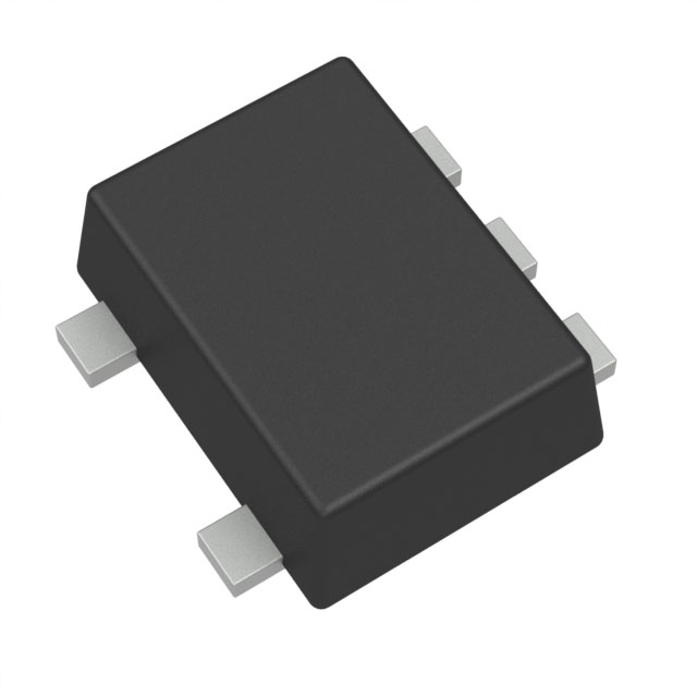
    The SN74LVC1G08DRLR is a member of the 74LVC1G series of logic gates, which are designed to provide high-speed performance with low power consumption. This device is available in a compact SOT-23 package, making it suitable for space-constrained applications.

    Features:

    1. Logic Function: Quad 2-input AND gate
    2. High-Speed Performance: Designed for high-speed operation, making it suitable for applications requiring rapid switching.
    3. Low Power Consumption: The device is designed to operate with low power, which is beneficial for battery-powered or energy-sensitive applications.
    4. Low Voltage Operation: It supports a wide range of supply voltages, making it versatile for different power supply environments.
    5. I/O Compatibility: The device features I/O compatibility with both 3.3V and 5V systems, allowing for easy integration into various systems.
    6. Small Package Size: The SOT-23 package is compact, making it suitable for applications where space is at a premium.

    Applications:

    1. Digital Logic Circuits: The SN74LVC1G08DRLR can be used to build various digital logic circuits due to its AND gate functionality.
    2. Automotive Applications: Its high-speed performance and low power consumption make it suitable for automotive electronics.
    3. Telecommunications: In high-speed communication systems, the device can be used for signal processing and control.
    4. Industrial Control Systems: The device can be used in control systems where high-speed logic operations are required.
    5. Consumer Electronics: It can be used in various consumer electronic devices, such as smartphones, tablets, and home appliances, for logic control and signal processing.
    6. IoT Devices: In Internet of Things (IoT) devices, the SN74LVC1G08DRLR can be used for logic operations and signal processing in a compact form factor.

    The SN74LVC1G08DRLR is a versatile device that can be used in a wide range of applications where high-speed performance, low power consumption, and compact packaging are required.

    Tech Specifications

    Unit Weight
    Maximum Propagation Delay Time @ Maximum CL (ns)
    Maximum Quiescent Current (uA)
    Product
    PPAP
    Automotive
    RoHS
    Maximum High Level Output Current (mA)
    Absolute Propagation Delay Time (ns)
    REACH Status
    Number of Inputs
    Output type
    Number of Element Outputs
    Maximum Operating Supply Voltage (V)
    Max Propagation Delay @ V, Max CL
    Operating temperature range (°C)
    Supplier Temperature Grade
    Standard Package Name
    High Level Output Current
    Mounting
    Input Logic Level - High
    Typical Operating Supply Voltage (V)
    Package
    IOH (max) (mA)
    Current - Output High, Low
    Output Type
    Process Technology
    Package Height
    Maximum Operating Temperature
    Width
    RoHS Status
    Current - Quiescent (Max)
    Number of channels
    Data rate (max) (Mbps)
    Number of Input Lines
    Number of Element Inputs
    Input Logic Level - Low
    Maximum Low Level Output Current (mA)
    Minimum Operating Temperature
    Number of Output Enables per Element
    Length
    Operating Supply Voltage
    Part Status
    Lead finish / Ball material
    Number of Circuits
    Package Width
    Supply voltage (min) (V)
    Product Status
    Supplier Package
    Package / Case
    Voltage - Supply
    Logic Function
    Inputs per channel
    EU RoHS
    Carrier
    Moisture Sensitivity Level (MSL)
    Operating Temperature
    Logic Type
    ECCN
    MSL rating / Peak reflow
    Mounting Type
    Pin Count
    Lead Shape
    Number of Gates
    Low Level Output Current
    HTSUS
    Pins
    USHTS
    Propagation Delay Time
    PCB changed
    HTS
    Number of Elements per Chip
    Rating
    ECCN (US)
    Supplier Device Package
    Supply Voltage - Min
    Minimum Operating Temperature (°C)
    Maximum Operating Temperature (°C)
    Function
    Propagation Delay Test Condition (pF)
    Mfr
    Supply voltage (max) (V)
    Features
    Height
    Number of Selection Inputs per Element
    Supply Voltage - Max
    Mounting Style
    Input Type
    Technology family
    Package Length
    REACH
    Series
    Input type
    Number of Output Lines
    IOL (max) (mA)
    Logic Family
    Base Product Number
    Minimum Operating Supply Voltage (V)

    SN74LVC1G08DRLR Documents

    Download datasheets and manufacturer documentation for SN74LVC1G08DRLR

    Ersa Logic Guide       SN74LVC1G08 Datasheet      
    Ersa Logic Guide      

    Shopping Guide

    Payment Methods
    Payment Methods include Prepayment TT (bank transfer), Western Union, and PayPal. Customers are responsible for shipping costs, bank charges, customs duties and taxes.
    Shipping Rate
    Shipments are made once a day around 5pm, excluding Sundays. Once shipped, the estimated delivery time is usually 5-7 business days, depending on the courier you choose.
    Delivery Methods
    Provide DHL, FedEx, UPS, EMS, SF Express and Registered Airmail International Delivery Service