
 German
 Japanese
 Portuguese
 Korea
Korea
 Mexico
 Dutch
Dutch


Texas Instruments
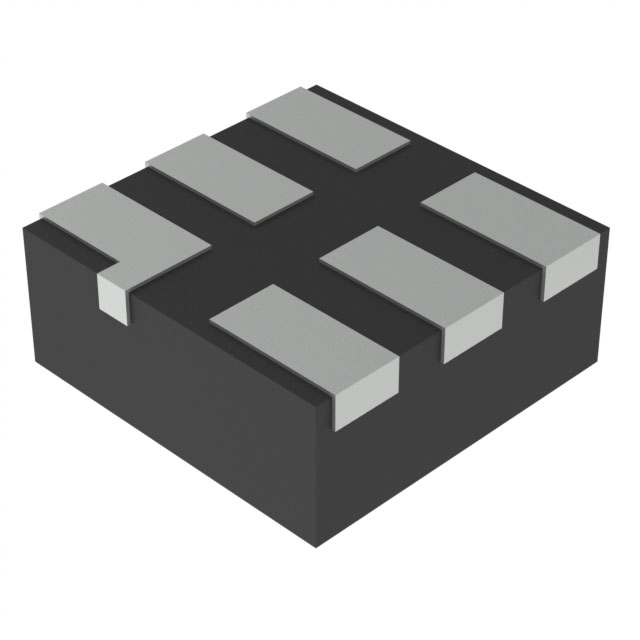
SN74LVC1G08DSF2

Why Choose Us?
Professional Platform
B2B & B2C purchasingDelivery at full speed
1-2 days deliveryWide variety
Original manufacturers365 days guarantee
Responsible quality
.png)


Tech Specifications
SN74LVC1G08DSF2 Description
SN74LVC1G08DSF2 Description
The SN74LVC1G08DSF2 is a high-performance, single-channel AND gate logic IC designed for a wide range of digital applications. Manufactured by Texas Instruments, this device is part of the 74LVC series, known for its robustness and versatility. The SN74LVC1G08DSF2 features a maximum propagation delay of 4ns at 5V and a maximum load capacitance of 50pF, ensuring rapid signal processing and high-speed performance. It operates within a supply voltage range of 1.65V to 5.5V, making it suitable for various power supply configurations.
SN74LVC1G08DSF2 Features
- Logic Type: AND Gate
- Number of Inputs: 2
- Number of Circuits: 1
- Max Propagation Delay: 4ns @ 5V, 50pF
- Voltage - Supply: 1.65V ~ 5.5V
- Current - Quiescent (Max): 10 µA
- Current - Output High, Low: 32mA, 32mA
- Mounting Type: Surface Mount
- Package: Tape & Reel (TR)
- Moisture Sensitivity Level (MSL): 1 (Unlimited)
- Compliance: ROHS3 Compliant, REACH Unaffected, ECCN: EAR99, HTSUS: 8542.39.0001
The SN74LVC1G08DSF2 offers several advantages over similar models. Its low quiescent current of 10 µA ensures minimal power consumption, making it ideal for battery-powered and energy-efficient applications. The device's ability to handle a maximum output current of 32mA for both high and low states provides strong drive capabilities, supporting a wide range of load conditions.
SN74LVC1G08DSF2 Applications
The SN74LVC1G08DSF2 is well-suited for a variety of applications due to its versatile design and performance characteristics. It is commonly used in digital signal processing, control systems, and data communication circuits. Specific use cases include:
- Digital Signal Processing: The fast propagation delay and robust performance make it ideal for processing high-speed digital signals in applications such as data converters and signal multiplexing.
- Control Systems: The AND gate functionality is essential for logic control in embedded systems, microcontrollers, and automation equipment.
- Data Communication Circuits: The device's ability to handle a wide range of supply voltages and its low quiescent current make it suitable for use in communication interfaces and networking equipment.
Conclusion of SN74LVC1G08DSF2
The SN74LVC1G08DSF2 is a versatile AND gate logic IC that offers high-speed performance, low power consumption, and robust operational characteristics. Its wide supply voltage range and strong drive capabilities make it suitable for a variety of applications, from digital signal processing to control systems. With its compliance to industry standards such as ROHS3 and REACH, the SN74LVC1G08DSF2 is an excellent choice for engineers and designers looking for reliable and efficient logic solutions.
FAQ
| Quantity | Unit Price | Ext. Price |
|---|---|---|
| 5+ | $0.17516 | $0.88 |
| 50+ | $0.13697 | $6.85 |
| 150+ | $0.12060 | $18.09 |
| 500+ | $0.10019 | $50.09 |
Not available to buy online? Want the lower wholesale price? Please Send RFQ to get best price, we will respond immediately


.png?x-oss-process=image/format,webp/resize,h_32)


