
 German
 Japanese
 Portuguese
 Korea
Korea
 Mexico
 Dutch
Dutch


Texas Instruments
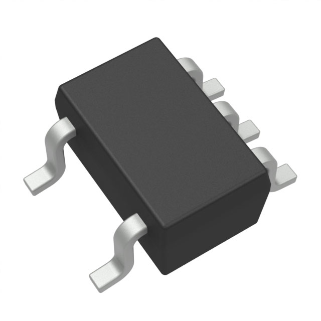
SN74LVC1G08MDCKREP

Why Choose Us?
Professional Platform
B2B & B2C purchasingDelivery at full speed
1-2 days deliveryWide variety
Original manufacturers365 days guarantee
Responsible quality
.png)


Tech Specifications
SN74LVC1G08MDCKREP Description
The SN74LVC1G08MDCKREP is a high-speed Si-gate CMOS device from Texas Instruments. It is a quad 2-input AND gate, which means it has four independent AND gates, each with two inputs. The device is designed to operate with a wide range of supply voltages, from 1.65V to 3.6V, making it suitable for a variety of applications.
Description:
The SN74LVC1G08MDCKREP is a member of the 1G08 series of logic gates from Texas Instruments. It is a quad 2-input AND gate, which means it has four independent AND gates, each with two inputs. The device is available in a small SOT-23 package, which is ideal for space-constrained applications.
Features:
- Quad 2-input AND gate configuration
- Wide operating voltage range: 1.65V to 3.6V
- High-speed performance: Propagation delay is 3.5 ns (typical) at a 3.3V supply voltage
- Low power consumption: 2.4 mA (typical) at a 3.3V supply voltage
- Available in a small SOT-23 package
Applications:
The SN74LVC1G08MDCKREP is suitable for a wide range of applications, including:
- Digital logic circuits: The device can be used to implement various digital logic functions, such as AND, OR, and NOT operations, in a compact form factor.
- Microcontroller input/output expansion: The device can be used to expand the number of digital input/output lines in a microcontroller-based system.
- Signal conditioning: The device can be used to condition digital signals, such as debouncing switches or removing noise from digital inputs.
- Data processing: The device can be used in data processing applications, such as digital filters or counters.
- Automotive electronics: The device's wide operating voltage range and high-speed performance make it suitable for use in automotive electronics, such as control modules or sensor interfaces.
In summary, the SN74LVC1G08MDCKREP is a versatile and compact quad 2-input AND gate from Texas Instruments, suitable for a wide range of digital logic and signal processing applications. Its high-speed performance, low power consumption, and small package size make it an attractive choice for designers working on space-constrained projects.
FAQ
| Quantity | Unit Price | Ext. Price |
|---|---|---|
| 1+ | $2.25280 | $2.25 |
| 10+ | $1.67376 | $16.74 |
| 25+ | $1.53014 | $38.25 |
| 100+ | $1.37174 | $137.17 |
| 250+ | $1.30332 | $325.83 |
Not available to buy online? Want the lower wholesale price? Please Send RFQ to get best price, we will respond immediately


.png?x-oss-process=image/format,webp/resize,h_32)


